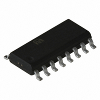
MIC2186BM Micrel Inc, MIC2186BM Datasheet - Page 14

MIC2186BM
Manufacturer Part Number
MIC2186BM
Description
IC PWM BST FLYBCK CM 16SOIC
Manufacturer
Micrel Inc
Datasheet
1.MIC2186YM.pdf
(15 pages)
Specifications of MIC2186BM
Pwm Type
Current Mode
Number Of Outputs
1
Frequency - Max
440kHz
Duty Cycle
85%
Voltage - Supply
2.9 V ~ 14 V
Buck
No
Boost
Yes
Flyback
Yes
Inverting
No
Doubler
No
Divider
No
Cuk
No
Isolated
No
Operating Temperature
-40°C ~ 125°C
Package / Case
16-SOIC (3.9mm Width)
Frequency-max
440kHz
Lead Free Status / RoHS Status
Contains lead / RoHS non-compliant
MIC2186
The output voltage is determined by the equation below.
Where: Vref for the MIC2186 is nominally 1.245V. Lower
values of resistance are preferred to prevent noise from
apprearing on the Vfb pin. A typically recommended value for
R1 is 10K.
Decoupling Capacitor Selection
The 1uf decoupling capacitor is used to stabilize the internal
regulator and minimize noise on the Vdd pin. Placement of
this capacitor is critical to the proper operation of the MIC2186.
It must be next to the Vdd and signal ground pins and routed
with wide etch. The capacitor should be a good quality
ceramic. Incorrect placement of the Vdd decoupling capaci-
tor will cause jitter and/or oscillations in the switching wave-
form as well as variations in the overcurrent limit.
A minimum 0.1uf ceramic capacitor is required to decouple
the Vin. The capacitor should be placed near the IC and
connected directly between pins 10 (Vcc) and 5 (SGND). A
0.1uf capacitor is required to decouple Vref. It should be
located near the Vref pin.
Efficiency calculation and considerations
Efficiency is the ratio of output power to input power. The
difference is dissipated as heat in the boost converter. The
significant contributors at light output loads are:
M9999-042205
* The VinA pin supply current.
* The VinP pin supply current which includes the
* Core losses in the inductor
To maximize efficiency at light loads:
* Use a low gate charge MOSFET or use the
V
current required to switch the external
MOSFETs
smallest MOSFET, which is still adequate for the
O
=
V
REF
× +
1
R2
R1
1.245V
Amplifier
Figure 11.
Voltage
MIC2186
V
REF
Pin
6
R1
R2
14
The significant contributors to power loss at higher output
loads are (in approximate order of magnitude):
To minimize power loss under heavy loads:
* Allow the MIC2186 to run in skip mode at lower
* se a ferrite material for the inductor core, which
* Resistive on-time losses in the MOSFET
* Switching transition losses in the MOSFET
* Inductor resistive losses
* Current sense resistor losses
* Output capacitor resistive losses (due to the
* Use Logic level, low on resistance MOSFETs.
* Slow transition times and oscillations on the
* For the same size inductor, a lower value will
* Lowering the current sense resistor value will
* Use low ESR output capacitors to minimize the
maximum output current.
currents. If running in PWM mode, set the
MIC2186 to switch at a lower frequency.
has less core loss than an MPP or iron power
core.
capacitor’s ESR)
Multiplying the gate charge by the on resistance
gives a figure of merit, providing a good balance
between switching and resistive power dissipa-
tion.
voltage and current waveforms dissipate more
power during the turn-on and turn-off of the low
side MOSFET. A clean layout will minimize
parasitic inductance and capacitance in the gate
drive and high current paths. This will allow the
fastest transition times and waveforms without
oscillations. Low gate charge MOSFETs will
switch faster than those with higher gate charge
specifications.
have fewer turns and therefore, lower winding
resistance. However, using too small of a value
will increase the inductor current and therefore
require more output capacitors to filter the output
ripple.
decrease the power dissipated in the resistor.
However, it will also increase the overcurrent
limit and may require larger MOSFETs and
inductor components to handle the higher
currents.
power dissipated in the capacitor’s ESR.
Micrel, Inc.
April 2005


