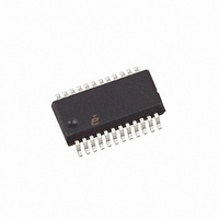
ISL6442IA Intersil, ISL6442IA Datasheet - Page 9

ISL6442IA
Manufacturer Part Number
ISL6442IA
Description
IC PWM BUCK VM 24QSOP
Manufacturer
Intersil
Datasheet
1.ISL6442IAZ-TK.pdf
(16 pages)
Specifications of ISL6442IA
Pwm Type
Voltage Mode
Number Of Outputs
3
Frequency - Max
2.85MHz
Duty Cycle
100%
Voltage - Supply
4.5 V ~ 24 V
Buck
Yes
Boost
No
Flyback
No
Inverting
No
Doubler
No
Divider
No
Cuk
No
Isolated
No
Operating Temperature
-40°C ~ 85°C
Package / Case
24-QSOP
Frequency-max
2.85MHz
Lead Free Status / RoHS Status
Contains lead / RoHS non-compliant
Available stocks
Company
Part Number
Manufacturer
Quantity
Price
Company:
Part Number:
ISL6442IAZ
Manufacturer:
Intersil
Quantity:
97
Company:
Part Number:
ISL6442IAZ
Manufacturer:
ST
Quantity:
6 267
Part Number:
ISL6442IAZ
Manufacturer:
INTERSIL
Quantity:
20 000
Part Number:
ISL6442IAZ-T
Manufacturer:
INTERSIL
Quantity:
20 000
Company:
Part Number:
ISL6442IAZ-TK
Manufacturer:
Intersil
Quantity:
6 000
Figure 8 shows pre-biased outputs before soft-start. The
solid blue curve shows no pre-bias; the output starts ramping
from GND. The magenta dotted line shows the output
pre-biased to a voltage less than the final output. The FETs
don’t turn on until the soft-start ramp voltage exceeds the
output voltage; then the output starts ramping seamlessly
from there. The cyan dotted line shows the output pre-
biased above the final output (but below the OVP
(Overvoltage Protection)). The FETs will not turn on until the
end of the soft-start ramp; then the output will be quickly
pulled down to the final value.
If the output is pre-biased above the OVP level, the ISL6442
will go into OVP at the end of soft-start, which will keep the
FETs off. The output can recover if the voltage goes below the
UV (Undervoltage) trip point, at which time a retry will occur. If
successful, the output will ramp back up to the normal level.
VOUT1 has the same functionality as previously described
for VOUT2. Each output should react independently of the
other, unless they are related by the circuit configuration.
NOTE: Neither output cannot be independently disabled during
power-up; both SS/EN pins are pulled low internally during POR, and
due to the internal switch, neither will start charging if either pin is still
held low. Once the outputs are running, either output can be disabled
and then enabled again, without affecting the other one that’s
running. But if both SS/EN pins are held low at the same time, then
the internal switch will turn on, and both SS/EN pins must be released
before they both start to ramp.
The linear output does not have a soft-start ramp; however, it
may follow the ramp of its input supply, if timed to coincide
with its rise, after the VCC rising POR trip. If the input to the
linear is from one of the two switcher outputs, then it will
share the same ramp rate as the switcher.
PGOOD
A group of comparators (separate from the protection
comparators) monitor the output voltages (via the FB pins)
for PGOOD. Each switcher has an lower and upper
boundary (nominally around 90% and 110% of the target
value) and the linear has a lower boundary (around 75% of
the target). Once both switcher output ramps are done, and
GND>
GND>
VOUT2 OVER-CHARGED
VOUT2 PRE-BIASED
FIGURE 8. SOFT-START WITH PRE-BIAS
SS2/EN2 (0.5V/DIV)
9
VOUT2 (2V/DIV)
ISL6442
all 3 outputs are within their expected ranges, the PGOOD
will start an internal timer, with Equation 3:
where:
t
F
Once the time-out is complete, the internal pull-down device
will shut off, allowing the open-drain PGOOD output to rise
through an external pull-up resistor, to a 5V (or lower) supply,
which signals that the “Power is GOOD”. Figure 9 shows the
three outputs turning on, and the delay for PGOOD. If any of
the conditions is subsequently violated, then PGOOD goes
low. Once the voltage returns to the normal region, a new
delay will start, after which the PGOOD will go high again.
The PGOOD delay is inversely proportional to the clock
frequency. If the clock is running as slow as 524kHz, the
delay will be one second long. There is no way to adjust the
PGOOD delay independently of the clock.
Monotonic Output
During soft-start period, the low side MOSFET is disabled to
achieve monotonic output voltage when the inductor current
is negative. This also allows ramping up into a pre-charged
output voltage.
Switching Frequency
The switching frequency of the ISL6442 is determined by the
external resistor placed from the RT pin to SGND. See
Figure 10 for a graph of Frequency versus RT Resistance.
The “Electrical Specifications” Table on page 5 lists a low
end value of 52.3kΩ for 300kHz operation (not shown on
graph). Running at both high frequency and high VIN
voltages is not recommended, due to the increased power
dissipation on-chip (mostly from the internal VCC regulator,
which supplies gate drivers). The user should check the
maximum acceptable IC temperature, based on their
particular conditions.
t
PGOOD
PGOOD
SW
GND>
GND>
GND>
GND>
is the switching frequency (in MHz)
is the delay time (in sec)
=
0.5236
----------------- -
F
SW
FIGURE 9. PGOOD DELAY
PGOOD (5V/DIV)
VOUT3 (2V/DIV)
VOUT2 (2V/DIV)
VOUT1 (2V/DIV)
October 31, 2008
(EQ. 3)
FN9204.2


