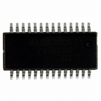
ISL6539IAZ Intersil, ISL6539IAZ Datasheet - Page 14

ISL6539IAZ
Manufacturer Part Number
ISL6539IAZ
Description
IC CTRLR DDR DRAM, SDRAM 28QSOP
Manufacturer
Intersil
Datasheet
1.ISL6539CAZ.pdf
(20 pages)
Specifications of ISL6539IAZ
Applications
Controller, DDR DRAM, SDRAM
Voltage - Input
3.3 ~ 18 V
Number Of Outputs
2
Voltage - Output
0.9 ~ 5.5 V
Operating Temperature
-40°C ~ 85°C
Mounting Type
Surface Mount
Package / Case
28-QSOP
Peak Reflow Compatible (260 C)
Yes
Rohs Compliant
Yes
Lead Free Status / RoHS Status
Lead free / RoHS Compliant
Available stocks
Company
Part Number
Manufacturer
Quantity
Price
Company:
Part Number:
ISL6539IAZ
Manufacturer:
Intersil
Quantity:
432
Company:
Part Number:
ISL6539IAZ
Manufacturer:
Intersil
Quantity:
156
Part Number:
ISL6539IAZ
Manufacturer:
INTERSIL
Quantity:
20 000
channel controller are disabled when the DDR pin is set
high. As the VTT channel tracks the VDDQ/2 voltage, the
soft-start function is not required, and the SOFT2 pin may be
left open, in the event both channels are enabled
simultaneously. However, if the VTT channel is enabled later
than the VDDQ, the SOFT2 pin must have a capacitor in
place to ensure soft-start. In case of overcurrent or
undervoltage caused by short circuit on VTT, the fault current
will propagate to the first channel and shut down the
converter.
The VREF voltage will be present even if the VTT is
disabled.
Channel Synchronization in DDR Applications
The presence of two PWM controllers on the same die
requires channel synchronization, to reduce inter-channel
interference that may cause the duty factor jitter and
increased output ripple.
The PWM controller is at greatest noise susceptibility when
an error signal on the input of the PWM comparator
approaches the decision-making point. False triggering may
occur, causing jitter and affecting the output regulation.
A common approach used to synchronize dual channel
converters is out-of-phase operation. Out-of-phase
operation reduces input current ripple and provides a
minimum interference for channels that control different
voltage levels.
When used in a DDR application with cascaded converters
(VTT generated from VDDQ), several methods of
synchronization are implemented in the ISL6539. When the
DDR pin is connected to GND for dual switcher applications,
the channels operate 180° out-of-phase. In the DDR mode,
when the DDR pin is connected to VCC, the channels
operate either with 0° phase shift, when the VIN pin is
connected to the GND, or with 90° phase shift if the VIN pin
is connected to a voltage higher than 4.2V.
The following table lists the different synchronization
schemes and their usage:
Application Information
Design Procedures
GENERAL
A ceramic decoupling capacitor should be used between the
VCC and GND pin of the chip. There are three major
currents drawn from the decoupling capacitor:
DDR PIN
0
1
1
V
V
V
IN
IN
IN
pin >4.2V
pin voltage <4.2V
pin voltage >4.1V
VIN PIN
14
180° out-of-phase
0° phase
90° phase shift
SYNCHRONIZATION
ISL6539
In order to reduce the noisy effect of the bootstrap capacitor
current to the IC, a small resistor, such as 10Ω, can be used
with the decoupling cap to construct a low pass filter for the
IC, as shown in Figure 11.
The soft-start capacitor and the resistor divider setting the
output voltage is easy to select as discussed in the “Block
Diagram” on page 8.
Selection of the Current Sense Resistor
The value of the current sense resistor determines the gain
of the current sensing circuit. It affects the current loop gain
and the overcurrent protection setpoint. The voltage drop on
the lower MOSFET is sensed within 400ns after the upper
MOSFET is turned off. The current sense pin has a 140Ω
resistor in series with the external current sensing resistor.
The current sense pin can source up to a 260µA current
while sensing current on the lower MOSFET, in such a way
that the voltage drop on the current sensing path would
equal to the voltage on the MOSFET.
I
worst case scenario, the high temperature r
increase to 150% of the room temperature level. During
overload condition, the MOSFET drain current I
130% higher than the normal inductor peak. If the inductor
has 30% peak-to-peak ripple, I
load current. The design should consider the above factors
so that the maximum I
under worst case conditions. To be safe, I
be less than 100µA in normal operation at room
temperature. The formula in the earlier discussion assumes
a 75µA sourcing current. Users can tune the sourcing
current of the ISEN pin to meet the overcurrent protection
and the change the current loop gain. The lower the current
sensing resistor, the higher gain of the current loop, which
can damp the output LC filter more.
A higher current-sensing resistor will decrease the current
sense gain. If the phase node of the converter is very noisy
due to poor layout, the sensed current will be contaminated,
resulting in duty cycle jittering by the current loop. In such a
case, a bigger current sense resistor can be used to reduce
both real and noise current levels. This can help damp the
phase node waveform jittering.
I
D
1. the quiescent current, supporting the internal logic and
2. the gate driver current for the lower MOSFETs
3. and the current going through the external diodes to the
SOURCING
can be assumed to be the inductor peak current. In a
normal operation of the IC
bootstrap capacitor for upper MOSFET.
FIGURE 11. INPUT FILTERING FOR THE CHIP
(
140Ω
5V
+
R
CS
SOURCING
TO BOOT
)
=
10Ω
I
D
r
DS ON
D
would equal to 115% of the
(
will not saturate to 260µA
)
VCC
SOURCING
DS(ON)
D
could be
April 29, 2010
could
(EQ. 16)
should
FN9144.6


