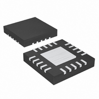
MAX8761ETG+ Maxim Integrated Products, MAX8761ETG+ Datasheet - Page 24

MAX8761ETG+
Manufacturer Part Number
MAX8761ETG+
Description
IC REG LINEAR LCD 24-TQFN
Manufacturer
Maxim Integrated Products
Datasheet
1.MAX8761ETG.pdf
(25 pages)
Specifications of MAX8761ETG+
Applications
Converter, LCD Power Supplies
Voltage - Input
8 ~ 28 V
Number Of Outputs
1
Voltage - Output
5V
Operating Temperature
0°C ~ 85°C
Mounting Type
Surface Mount
Package / Case
24-TQFN Exposed Pad
Lead Free Status / RoHS Status
Lead free / RoHS Compliant
Low-Cost, Linear-Regulator
LCD Panel Power Supplies
Careful PC board layout is important for proper opera-
tion. Use the following guidelines for good PC board
layout:
1) Create a power ground island consisting of the lin-
2) Place all feedback voltage-divider resistors as close
3) Place IN, INL, SUPB, SUPCP, and REF pin bypass
4) Minimize the length and maximize the width of the
5) Minimize the size of the switching nodes (DRVP and
Refer to the MAX8710 evaluation kit for an example of
proper board layout.
24
ear-regulator input and output-capacitor ground
connections, the GND pin, and the capacitor
ground connections for the charge-pump regula-
tors. Connect all these together with short, wide
traces or a small ground plane. Maximizing the
width of the power ground traces improves efficien-
cy. Create an analog ground island consisting of all
the feedback-divider ground connections, the oper-
ational-amplifier divider ground connection, the REF
capacitor ground connection, the MODE capacitor
ground connection, the DLP capacitor ground con-
nection, and the device’s exposed backside pad.
Connect the analog ground island and the power
ground island by connecting the GND pin directly to
the exposed backside pad. Make no other connec-
tions between these separate ground islands.
to their respective feedback pins as possible. The
divider’s center trace should be kept short. Placing
the resistors far away causes their FB traces to
become antennas that can pick up noise from the
switching nodes of the charge pumps. Avoid running
any feedback trace near these switching nodes.
capacitors close to the IC. The ground connection
of the IN bypass capacitor should be connected
directly to the GND pin with a wide trace.
traces between the output capacitors and the load
for best transient responses.
DRVN). Keep the switching nodes away from feed-
back nodes (FBL, FBP, and FBN) and the analog
ground. Use DC traces as a shield if necessary.
______________________________________________________________________________________
PC Board Layout Guidelines
MAX8710/MAX8711/MAX8712 TRANSISTOR COUNT:
3946
MAX8761 TRANSISTOR COUNT: 4127
PROCESS: BiCMOS
TOP VIEW
Pin Configurations (continued)
SHDN
DLP
FBN
FBL
DLP
FBN
FBL
13
14
15
16
11
12
10
+
+
THIN QFN 4mm x 4mm
THIN QFN 4mm x 4mm
12
1
9
1
MAX8711
MAX8712
11
2
8
2
Chip Information
10
3
7
3
9
4
6
5
4
8
7
6
5
DRVP
DRVN
OUTL
DRVP
DRVN
OUTL
IN


