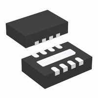
LTC3408EDD Linear Technology, LTC3408EDD Datasheet - Page 8

LTC3408EDD
Manufacturer Part Number
LTC3408EDD
Description
IC REG BUCK W/BYPASS TXRX 8-DFN
Manufacturer
Linear Technology
Datasheet
1.LTC3408EDD.pdf
(12 pages)
Specifications of LTC3408EDD
Applications
Converter, WCDMA Power Amplifier Applications
Voltage - Input
2.5 ~ 5 V
Number Of Outputs
1
Voltage - Output
0.3 ~ 3.5 V
Operating Temperature
-40°C ~ 85°C
Mounting Type
Surface Mount
Package / Case
8-DFN
Lead Free Status / RoHS Status
Contains lead / RoHS non-compliant
Available stocks
Company
Part Number
Manufacturer
Quantity
Price
Company:
Part Number:
LTC3408EDD
Manufacturer:
LINEAR
Quantity:
50
APPLICATIO S I FOR ATIO
At output voltages below 0.6V, the switching frequency
decreases linearly to a minimum of approximately 700kHz.
This places the maximum ripple current (in forced con-
tinuous mode) at the highest input voltage and the lowest
output voltage. In practice, the resulting ouput ripple
voltage is 10mV to 15mV using the components specified
in Figure 1.
The DC current rating of the inductor should be at least equal
to the maximum load current plus half the ripple current to
prevent core saturation. Thus, a 660mA rated inductor
should be enough for most applications (600mA + 60mA).
For better efficiency, choose a low DC-resistance inductor.
Inductor Core Selection
Different core materials and shapes will change the size/
current and price/current relationship of an inductor.
Toroid or shielded pot cores in ferrite or permalloy mate-
rials are small and don’t radiate much energy but generally
cost more than powdered iron core inductors with similar
electrical characteristics. The choice of which style induc-
tor to use often depends more on the price versus size
requirements and any radiated field/EMI requirements
than on what the LTC3408 requires to operate. Table 1
shows some typical surface mount inductors that work
well in LTC3408 applications.
Table 1. Representative Surface Mount Inductors
PART
NUMBER
Sumida
CDRH2D11
Sumida
CDRH2D18/LD
Sumida
CMD4D06
Murata
LQH32C
Taiyo Yuden
LBLQ2016
Toko
D312C
C
In continuous mode, the source current of the top MOSFET
is a square wave of duty cycle V
voltage transients, a low ESR input capacitor sized for the
LTC3408
8
IN
and C
OUT
Selection
VALUE
(µH)
4.7
4.7
4.7
4.7
4.7
4.7
U
(ΩMAX)
0.135
0.078
0.216
0.150
0.250
DCR
0.20
U
CURRENT (A) WxLxH (mm
OUT
MAX DC
W
0.210
/V
0.63
0.75
0.65
0.79
0.5
IN
. To prevent large
3.2 x 3.2 x 1.2
3.2 x 3.2 x 2.0
3.5 x 4.1 x 0.8
2.5 x 3.2 x 2.0
1.6 x 2.0 x 1.6
3.6 x 3.6 x 1.2
U
SIZE
3
)
maximum RMS current must be used. The maximum
RMS capacitor current is given by:
This formula has a maximum at V
= I
used for design because even significant deviations do not
offer much relief. Note that the capacitor manufacturer’s
ripple current ratings are often based on 2000 hours of life.
This makes it advisable to further derate the capacitor, or
choose a capacitor rated at a higher temperature than re-
quired. Always consult the manufacturer if there is any
question.
The selection of C
series resistance (ESR). Typically, once the ESR
requirement for C
rating generally far exceeds the I
The output ripple V
where f = operating frequency, C
and I
voltage, the output ripple is highest at maximum input
voltage since I
Aluminum electrolytic and dry tantalum capacitors are
both available in surface mount configurations. In the case
of tantalum, it is critical that the capacitors are surge tested
for use in switching power supplies. An excellent choice is
the AVX TPS series of surface mount tantalum. These are
specially constructed and tested for low ESR so they give
the lowest ESR for a given volume. Other capacitor types
include Sanyo POSCAP, Kemet T510 and T495 series, and
Sprague 593D and 595D series. Consult the manufacturer
for other specific recommendations.
The bulk capacitance values in Figure 1(a) (C
C
which the output voltage is expected to slew quickly
according to the needs of the power amplifier. Holding the
output capacitor to 4.7µF facilitates rapid charging and
discharging. When the output voltage descends quickly in
OUT
OUT
C required I
∆
IN
V
L
= 4.7µF) are tailored to mobile phone applications, in
OUT
/2. This simple worst-case condition is commonly
= ripple current in the inductor. For a fixed output
≅ ∆
L
I ESR
L
increases with input voltage.
RMS
OUT
OUT
OUT
≅
is driven by the required effective
+
has been met, the RMS current
I
is determined by:
OMAX
8
f C
1
OUT
[
V
OUT
RIPPLE(P-P)
OUT IN
IN
= 2V
= output capacitance
(
V
V
OUT
–
IN
V
requirement.
, where I
OUT
IN
)]
= 10µF,
/ 1 2
RMS
3408f


