LT1947EMS Linear Technology, LT1947EMS Datasheet
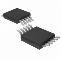
IC SW REG TFT-LCD TRPL ADJ10MSOP

LT1947EMS

Manufacturer Part Number
LT1947EMS
Description
IC SW REG TFT-LCD TRPL ADJ10MSOP
Manufacturer
Linear Technology
Datasheet

Specifications of LT1947EMS

Applications
Converter, TFT, LCD
Voltage - Input
2.7 ~ 8 V
Number Of Outputs
3
Voltage - Output
Adjustable up to 30V
Operating Temperature
-40°C ~ 85°C
Mounting Type
Surface Mount
Package / Case
10-MSOP, Micro10™, 10-uMAX, 10-uSOP
Lead Free Status / RoHS Status
Contains lead / RoHS non-compliant

Available stocks

Company
Part Number
Manufacturer
Quantity
Price
Part Number:
LT1947EMS
Manufacturer:
LT
Quantity:
10 000
Part Number:
LT1947EMS
Manufacturer:
LT
Quantity:
1 000
Part Number:
LT1947EMS
Manufacturer:
LT
Quantity:
4 794
Part Number:
LT1947EMS
Manufacturer:
LT/凌特
Quantity:
20 000
Part Number:
LT1947EMS#PBF
Manufacturer:
MAX
Quantity:
4
Part Number:
LT1947EMS#PBF
Manufacturer:
LINEAR/凌特
Quantity:
20 000
Part Number:
LT1947EMS#TR
Manufacturer:
LINEAR/凌特
Quantity:
20 000
Part Number:
LT1947EMS#TRPBF
Quantity:
6 225
Part Number:
LT1947EMS#TRPBF
Manufacturer:
LINEAR/凌特
Quantity:
20 000
Part Number:
LT1947EMSE
Manufacturer:
LT
Quantity:
10 000
Part Number:
LT1947EMSE
Manufacturer:
LINEAR/凌特
Quantity:
20 000
FEATURES
APPLICATIO S
SHUTDOWN
TYPICAL APPLICATIO
Complete Solution Under 1.2mm
Develops Three Outputs from a 3.3V or 5V Supply
Externally Programmable V
Fixed Frequency Low Noise Outputs
All Ceramic Capacitors
3MHz Switching Frequency
Fast Transient Response
Few External Components Required
2.7V to 8V Input Range
Adjustable AV
Tiny 10-Lead MSOP and Thermally Enhanced
10-Lead MSOP Packages
TFT-LCD Notebook Display Panels
TFT-LCD Desktop Monitor Display Panels
Digital Cameras
Handheld Computers
CERAMIC
C1: TAIYO YUDEN LMK316BJ225MD
C2: TAIYO YUDEN LMK325BJ335MD ×2
C3: AVX 0.22µF 25V X7R
C4, C6: TAIYO YUDEN LMK107BJ684MA
2.2µF
V
IN
C1
Figure 1. 3.3V Powered TFT-LCD Bias Generator
DD
L2
4.7µH
D2
C3
220nF
U
and V
R3
182k
R4
10k
ON
Voltages
SW2
V
FB2
ON
O2
SHDN C
10nF
V
IN
C5
Delay
LT1947
D1: MBRM120LT3
D2: CMDSH-3
D3, D4: BAT54S DUAL DIODE
L1: SUMIDA CLQ4D103R3
L2: TAIYO YUDEN LB2012B4R7M
3.3µH
U
L1
T
D3
SW1
GND
V
FB1
ON
D1
C6
0.68µF
D4
R1
53.6k
R2
10k
1947 F01
C4
0.68µF
CERAMIC
C2
3.3µF
CERAMIC
×2
AV
8V
200mA
V
–8V
10mA
V
24V
10mA
OFF
ON
DD
Adjustable Output TFT-LCD
DESCRIPTIO
The LT
converter designed for use in TFT-LCD panels. The device
contains two independent switching regulators. The main
regulator has an adjustable output voltage with an internal
1.1A switch that can generate a boosted voltage as high as
30V. The second regulator’s output is also adjustable up
to 30V and can deliver 10mA for positive bias. A simple
level-shift charge pump off the main switch node gener-
ates the negative bias voltage. An external capacitor sets
the delay time from AV
the V
of tiny low profile chip inductors and capacitors through-
out, providing a low noise, low cost total solution with all
components under 1.2mm in height. The device operates
from an input range of 2.7V to 8V and is available in
10-lead MSOP and thermally enhanced 10-lead MSOP
packages.
All other trademarks are the property of their respective owners.
Triple Switching Regulator
, LTC and LT are registered trademarks of Linear Technology Corporation.
ON
®
1947 is a highly integrated multiple output DC/DC
pin. The 3MHz switching frequency allows the use
20V/DIV
10V/DIV
10V/DIV
5V/DIV
V
AV
SHDN
V
V
OFF
ON
DD
U
DD
’s final value to the rising edge at
Start-Up Waveforms
2ms/DIV
LT1947
1947 TA01.tif
1947fa
1

Related parts for LT1947EMS

LT1947EMS Summary of contents

Page 1

... The device operates from an input range of 2. and is available in 10-lead MSOP and thermally enhanced 10-lead MSOP packages. , LTC and LT are registered trademarks of Linear Technology Corporation. All other trademarks are the property of their respective owners OFF – ...

Page 2

... PLASTIC MSOP T JMAX LTBQW The ● denotes the specifications which apply over the full operating = 25° 3.3V SHDN = 2. ORDER PART NUMBER TOP VIEW LT1947EMS SHDN 7 SW2 PART MARKING = 125°C, θ = 120°C/W JA LTUE = 3.3V unless otherwise specified. MIN TYP 2 ...

Page 3

ELECTRICAL CHARACTERISTICS temperature range, otherwise specifications are at T SYMBOL CONDITIONS Error Amplifier Voltage Gain EA1 and EA2 C Current Source V T FB1 C Threshold to Turn FB1 Voltage to Begin C Charge T SW1 Current ...

Page 4

LT1947 W U TYPICAL PERFOR A CE CHARACTERISTICS SW1 Current Limit 1.8 1.6 1.4 1.2 1.0 0.8 –50 – TEMPERATURE (°C) Switch 1 Saturation Voltage 500 400 25°C 300 90°C 200 –45°C 100 0 0 0.2 0.4 0.6 ...

Page 5

CTIO S FB1 (Pin 1): Feedback Pin for First Switcher. Connect resistor divider tap here. Set 1.26V(1 + R1/R2). DD FB2 (Pin 2): Feedback Pin for Second Switcher. Connect resistor divider 2 ...

Page 6

LT1947 W BLOCK DIAGRA – REF V O2 OSC 1.26V REFERENCE 3MHz AND SLOPE 1 OSCILLATOR UNDERVOLTAGE SLOPE 2 LOCKOUT 6 – FB1 5.5µA 28mV + – + – REF + REF – ...

Page 7

U OPERATIO To best understand operation of the LT1947, please refer to the LT1947 Block Diagram. The device contains two switching regulators, a timer and a high side switch. Three outputs can be generated: an adjustable AV charge-pumped inversion of ...

Page 8

LT1947 U OPERATIO V 2.2µF CERAMIC R SS 33. 33nF C1: TAIYO YUDEN LMK316BJ225MD C2: TAIYO YUDEN LMK325BJ335MD ×2 C3: AVX 0.22µF 25V X7R C4, C6: TAIYO YUDEN LMK107BJ684MA 5V/DIV 20V/DIV AV 10V/DIV 10V/DIV 8 D3 ...

Page 9

U TYPICAL APPLICATIO 3.3V C1 4.7µF SHUTDOWN C1: TAIYO YUDEN JMK316BJ475MD 4.7µF 6.3V X7R C2: TAIYO YUDEN LMK325BJ335MD 3.3µF 10V X7R ×2 C3: AVX 0.22µF 25V X7R C4, C6: TAIYO YUDEN LMK107BJ684MA 0.68µF 10V X7R V IN ...

Page 10

LT1947 PACKAGE DESCRIPTIO 5.23 (.206) MIN 0.305 ± 0.038 (.0120 ± .0015) TYP RECOMMENDED SOLDER PAD LAYOUT 0.254 (.010) GAUGE PLANE 0.18 (.007) NOTE: 1. DIMENSIONS IN MILLIMETER/(INCH) 2. DRAWING NOT TO SCALE 3. DIMENSION DOES NOT INCLUDE MOLD FLASH, ...

Page 11

... LEAD COPLANARITY (BOTTOM OF LEADS AFTER FORMING) SHALL BE 0.102mm (.004") MAX Information furnished by Linear Technology Corporation is believed to be accurate and reliable. However, no responsibility is assumed for its use. Linear Technology Corporation makes no represen- tation that the interconnection of its circuits as described herein will not infringe on existing patent rights. ...

Page 12

... MS10 OUT Q SHDN Max = 6V 38µ <1µA, MS10 OUT Q SHDN Max = 6V 38µ <1µA, MS10 OUT Q SHDN Max = 6V 38µ <1µA, MS10 OUT Q SHDN LT/LT 0605 REV A • PRINTED IN USA © LINEAR TECHNOLOGY CORPORATION 2001 1947fa ...

Related keywords