LTC3450EUD Linear Technology, LTC3450EUD Datasheet
LTC3450EUD
Specifications of LTC3450EUD
Available stocks


Related parts for LTC3450EUD


LTC3450EUD Summary of contents
Page 1
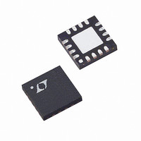
... LCD panel. The LTC3450 is offered in a low profile (0.75mm), 3mm × 3mm 16-pin QFN package, minimizing the solution profile and footprint. , LTC and LT are registered trademarks of Linear Technology Corporation. All other trademarks are the property of their respective owners 5.1V/10mA 2.2µ ...
Page 2
... MODE = GND SHDN = GND, V OPEN OUT Load 5mA OUT Load 5mA, (Note 2) OUT L = 47µH, (Note 2) MODE = V IN MODE = GND Load on V2X = 100µ ORDER PART NUMBER LTC3450EUD 12 V2X + 11 C1 – GND 9 UD PART MARKING 8 LAAC (PIN 17) NEG = 68°C/W JA MIN TYP ...
Page 3
ELECTRICAL CHARACTERISTICS temperature range, otherwise specifications are at T PARAMETER V3X Output Voltage V2X Efficiency V3X Efficiency Output Impedance V2X, V3X V Output Voltage NEG V Efficiency NEG Output Impedance V NEG Switching Frequency Charge Pumps Switching Frequency Charge Pumps ...
Page 4
LTC3450 W U TYPICAL PERFOR A CE CHARACTERISTICS AV Efficiency 100 L = 100µ 1.5 2.0 2.5 No Load V Current in Blank Mode IN 100 ...
Page 5
W U TYPICAL PERFOR A CE CHARACTERISTICS AV Ripple Voltage DD AV Load = 5mA 5mV/DIV (AC 3.6V 1µs/DIV 2.2µ Turn-On and Turn-Off Sequence ...
Page 6
LTC3450 CTIO (Pin 1): Charge Pump Inverter Flying Capacitor Posi- tive Node. The charge pump inverter flying capacitor is + – connected between C3 and C3 . The voltage on C3 alternate ...
Page 7
CTIO S V3X (Pin 15): Charge Pump Tripler Output. This output is 15.3V (nom load and is capable of delivering up to 500µ load. V3X should be bypassed to GND with ...
Page 8
LTC3450 U OPERATIO The LTC3450 is a highly integrated power converter in- tended for small TFT-LCD display modules. A fixed fre- quency, synchronous PWM boost regulator generates a low noise 5.1V, 10mA bias at greater than 90% efficiency from an ...
Page 9
U U APPLICATIO S I FOR ATIO Inductor Selection Inductors in the range of 47µH to 100µH with saturation current (I ) ratings of at least 150mA are recommended SAT for use with the LTC3450. Ferrite core materials are strongly ...
Page 10
LTC3450 U U APPLICATIO S I FOR ATIO MODE SHDN NOTE: QFN PACKAGE EXPOSED PAD IS CONNECTED TO THE V DO NOT CONNECT EXPOSED PAD TO GROUND U TYPICAL APPLICATIO 4.6V 2.2µF BLANK SCAN OFF ...
Page 11
... SHADED AREA IS ONLY A REFERENCE FOR PIN 1 LOCATION ON THE TOP AND BOTTOM OF PACKAGE Information furnished by Linear Technology Corporation is believed to be accurate and reliable. However, no responsibility is assumed for its use. Linear Technology Corporation makes no represen- tation that the interconnection of its circuits as described herein will not infringe on existing patent rights Package 16-Lead Plastic QFN (3mm × ...
Page 12
... I = 9.5mA <1µA OUT 28V 4.5mA <25µA OUT 5V 19µA/300µ <1µA OUT 5V 38µ <1µA, MS Package OUT 5V 38µ <1µA, MS Package OUT Q SD LT/TP 0205 1K REV A • PRINTED IN USA © LINEAR TECHNOLOGY CORPORATION 2003 3450fa ...