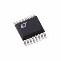
LTC3717EGN Linear Technology, LTC3717EGN Datasheet - Page 11

LTC3717EGN
Manufacturer Part Number
LTC3717EGN
Description
IC STEP-DWN CONTRLR SYNC 16-SSOP
Manufacturer
Linear Technology
Datasheet
1.LTC3717EGN.pdf
(20 pages)
Specifications of LTC3717EGN
Applications
Controller, DDR, QDR
Voltage - Input
4 ~ 36 V
Number Of Outputs
1
Voltage - Output
2 ~ 18 V
Operating Temperature
-40°C ~ 85°C
Mounting Type
Surface Mount
Package / Case
16-SSOP
Lead Free Status / RoHS Status
Contains lead / RoHS non-compliant
Available stocks
Company
Part Number
Manufacturer
Quantity
Price
Part Number:
LTC3717EGN
Manufacturer:
LT/凌特
Quantity:
20 000
Company:
Part Number:
LTC3717EGN#PBF
Manufacturer:
LT
Quantity:
416
Part Number:
LTC3717EGN#TRPBF
Manufacturer:
LT/凌特
Quantity:
20 000
APPLICATIO S I FOR ATIO
current ratings from capacitor manufacturers are often
based on only 2000 hours of life which makes it advisable
to derate the capacitor.
The selection of C
required to minimize voltage ripple and load step
transients. The output ripple V
bounded by:
Since I
highest at maximum input voltage. Typically, once the ESR
requirement is satisfied, the capacitance is adequate for
filtering and has the necessary RMS current rating.
Multiple capacitors placed in parallel may be needed to
meet the ESR and RMS current handling requirements.
Dry tantalum, special polymer, aluminum electrolytic and
ceramic capacitors are all available in surface mount
packages. Special polymer capacitors offer very low ESR
but have lower capacitance density than other types.
Tantalum capacitors have the highest capacitance density
but it is important to only use types that have been surge
tested for use in switching power supplies. Aluminum
electrolytic capacitors have significantly higher ESR, but
can be used in cost-sensitive applications providing that
consideration is given to ripple current ratings and long
term reliability. Ceramic capacitors have excellent low
ESR characteristics but can have a high voltage coefficient
and audible piezoelectric effects. The high Q of ceramic
capacitors with trace inductance can also lead to signifi-
cant ringing. When used as input capacitors, care must be
taken to ensure that ringing from inrush currents and
switching does not pose an overvoltage hazard to the
power switches and controller. To dampen input voltage
transients, add a small 5 F to 50 F aluminum electrolytic
capacitor with an ESR in the range of 0.5 to 2 . High
performance through-hole capacitors may also be used,
but an additional ceramic capacitor in parallel is recom-
mended to reduce the effect of their lead inductance.
Top MOSFET Driver Supply (C
An external bootstrap capacitor C
pin supplies the gate drive voltage for the topside MOSFET.
V
OUT
L
increases with input voltage, the output ripple is
I ESR
L
OUT
U
is primarily determined by the ESR
8
U
fC
1
OUT
B
B
, D
connected to the BOOST
OUT
W
B
)
is approximately
U
This capacitor is charged through diode D
when the switch node is low. When the top MOSFET turns
on, the switch node rises to V
to approximately V
to store about 100 times the gate charge required by the
top MOSFET. In most applications 0.1 F to 0.47 F, X5R or
X7R dielectric capacitor is adequate.
Fault Condition: Current Limit
The maximum inductor current is inherently limited in a
current mode controller by the maximum sense voltage. In
the LTC3717, the maximum sense voltage is controlled by
the voltage on the V
the maximum sense voltage and the sense resistance
determine the maximum allowed inductor valley current.
The corresponding output current limits are:
The current limit value should be checked to ensure that
I
generally occurs with the largest V
ent temperature, conditions that cause the largest power
loss in the converter. Note that it is important to check for
self-consistency between the assumed MOSFET junction
temperature and the resulting value of I
the MOSFET switches.
Caution should be used when setting the current limit
based upon the R
current limit is determined by the minimum MOSFET on-
resistance. Data sheets typically specify nominal and
maximum values for R
reasonable assumption is that the minimum R
the same amount below the typical value as the maximum
lies above it. Consult the MOSFET manufacturer for further
guidelines.
Minimum Off-time and Dropout Operation
The minimum off-time t
LIMIT(MIN)
I
I
LIMIT
LIMIT
NEGATIVE
POSITIVE
> I
OUT(MAX)
DS(ON)
IN
RNG
+ INTV
. The minimum value of current limit
R
R
V
OFF(MIN)
V
DS ON
SNS MAX
DS ON
DS(ON)
of the MOSFETs. The maximum
pin. With valley current control,
SNS MIN
(
(
CC
(
(
)
. The boost capacitor needs
IN
)
, but not a minimum. A
is the smallest amount of
and the BOOST pin rises
)
)
T
T
IN
–
at the highest ambi-
2
2
1
1
LIMIT
I
I
LTC3717
L
L
B
from INTV
which heats
DS(ON)
sn3717 3717fs
11
lies
CC


