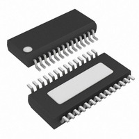
MAX8538EEI+T Maxim Integrated Products, MAX8538EEI+T Datasheet - Page 8

MAX8538EEI+T
Manufacturer Part Number
MAX8538EEI+T
Description
IC CNTRLR BUCK DUAL 28-QSOP
Manufacturer
Maxim Integrated Products
Datasheet
1.MAX8538EEI.pdf
(23 pages)
Specifications of MAX8538EEI+T
Applications
Controller, DDR
Voltage - Input
4.5 ~ 23 V
Number Of Outputs
2
Voltage - Output
0.8 ~ 3.6 V
Operating Temperature
0°C ~ 85°C
Mounting Type
Surface Mount
Package / Case
28-QSOP
Output Voltage
0.8 V to 3.6 V
Output Current
30 A
Input Voltage
4.5 V to 23 V
Mounting Style
SMD/SMT
Maximum Operating Temperature
+ 85 C
Minimum Operating Temperature
- 40 C
Lead Free Status / RoHS Status
Lead free / RoHS Compliant
The MAX8537/MAX8539 controllers provide a complete
power-management solution for both DDR and combin-
er supplies. The MAX8537 and MAX8539 are config-
ured for out-of-phase and in-phase DDR power-supply
operations, respectively. In addition to the dual-syn-
chronous buck controllers, they also contain an addi-
tional amplifier to generate a total of three outputs: the
main memory voltage (V
sinking/sourcing termination voltage (V
mination reference voltage (V
configured as a dual out-of-phase controller for point-
of-load supplies. Each buck controller can source or
sink up to 25A of current, while the termination refer-
ence can supply up to 15mA output.
The MAX8537/MAX8539 have a 1% accurate refer-
ence. The first buck controller generates V
external resistor-dividers. The second synchronous
buck controller and the amplifier generate 1/2 V
voltage for V
are maintained within 1% of 1/2 V
The MAX8537/MAX8538/MAX8539 use a constant-fre-
quency voltage-mode architecture with operating fre-
quencies of 200kHz to 1.4MHz to allow flexible design.
Dual-Synchronous Buck Controllers for Point-of-
Load, Tracking, and DDR Memory Power Supplies
8
_______________________________________________________________________________________
PIN
22
23
24
25
26
27
28
TT
(MAX8537/
MAX8539)
and V
NAME
PGND
ILIM1
BST1
DH1
DL1
LX1
VL
TTR
Detailed Description
. The V
(MAX8538)
NAME
PGND
ILIM1
BST1
DH1
DL1
LX1
VL
DDQ
TTR
DDQ
TT
). The MAX8538 is
and V
), the tracking
.
TT
Internal 5V Linear Regulator to Power the IC. VL is always on. Bypass with a ceramic
capacitor with 1µF/10mA of load current. The internal VL regulator can be disabled by
connecting VL and V+ to an externally generated 5V. VL output current can be
boosted with an external PNP transistor.
Low-Side Gate-Driver Output for Step-Down 1. Swings from PGND to VL.
Power Ground for Gate-Driver Circuits
Output Current-Limit Setting for Step-Down 1. Connect a resistor from ILIM1 to the
drain of the step-down 1 high-side MOSFET, or to the junction of the source of the
high-side MOSFET and the current-sense resistor to set the current-limit threshold.
See the Current-Limit Setting section.
External Inductor Input for Step-Down 1. Connect to the switched side of the inductor.
LX1 serves as the lower supply-voltage rail for the DH1 high-side gate driver and
current-limit circuitry.
High-Side Gate-Driver Step-Down 1. Swings from LX1 to BST1.
Bootstrap Input to Power Internal High-Side Driver for Step-Down 1. Connect to an
external capacitor and diode according to Figure 1.
), and the ter-
TTR
DDQ
voltages
using
DDQ
An internal high-bandwidth (25MHz) operational ampli-
fier is used as an error amplifier to regulate the output
voltage. This allows fast transient response, reducing
the number of output capacitors. Synchronous rectifica-
tion ensures high efficiency and balanced current
sourcing and sinking capability for V
design optimizes efficiency and cost. The two convert-
ers can be operated in-phase or out-of-phase to mini-
mize capacitance and optimize performance for all
V
Both channels have independent enable and power-
good functions. They also have high-side current-sense
architectures. ILIM pins allow the setting of an
adjustable, lossless current limit for different combina-
tions of load current and R
rate overcurrent protection is achieved by using a
sensing resistor in series with the high-side FET. The
positive current-limit threshold is programmable
through an external resistor. Overvoltage protection is
achieved by latching off the high-side MOSFET and
latching on the low-side MOSFET when the output volt-
age exceeds 17% of its set output.
IN
/V
OUT
combinations.
Pin Description (continued)
FUNCTION
DS(ON)
. Additionally, accu-
TT
. An all-N-FET


