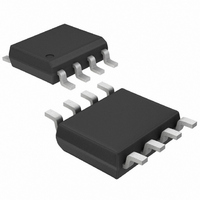
MAX844ESA+ Maxim Integrated Products, MAX844ESA+ Datasheet - Page 2

MAX844ESA+
Manufacturer Part Number
MAX844ESA+
Description
IC BIAS GAASFET REG 8-SOIC
Manufacturer
Maxim Integrated Products
Datasheet
1.MAX844ISA.pdf
(10 pages)
Specifications of MAX844ESA+
Applications
Charge Pump, Cellular Telephone Transmitter
Voltage - Input
2.5 ~ 10 V
Number Of Outputs
1
Voltage - Output
-2V
Operating Temperature
-40°C ~ 85°C
Mounting Type
Surface Mount
Package / Case
8-SOIC (3.9mm Width)
Function
Inverting
Output Voltage
- 2 V, - 0.5 V to - 9.4 V
Output Current
4 mA
Maximum Operating Temperature
+ 85 C
Minimum Operating Temperature
- 40 C
Mounting Style
SMD/SMT
Lead Free Status / RoHS Status
Lead free / RoHS Compliant
ABSOLUTE MAXIMUM RATINGS
Supply Voltage, V
V
V
V
V
Continuous Power Dissipation (T
Low-Noise, Regulated, -2V GaAsFET Bias
ELECTRICAL CHARACTERISTICS
(Figures 2a and 2c, 2.5V ≤ V
Typical values are measured at V
Note 1:
Stresses beyond those listed under “Absolute Maximum Ratings” may cause permanent damage to the device. These are stress ratings only, and functional
operation of the device at these or any other conditions beyond those indicated in the operational sections of the specifications is not implied. Exposure to
absolute maximum rating conditions for extended periods may affect device reliability.
2
NEGOUT
IN
OUT
Supply Voltage Range
Output Voltage
Output Voltage Adjust Range
FB Voltage
FB Leakage Current
CONT Leakage Current
Supply Current
Shutdown Supply Current
V
V
Oscillator Frequency
Input High Voltage
Input Low Voltage
Input Current
Input Capacitance
SHDN
SO (derate 5.88mW/°C above +70°C) .........................471mW
OUT
OUT
to V
_______________________________________________________________________________________
to GND (Note 1).......................................V
Load Regulation
Ripple
NEGOUT
to GND ............................................-0.3V to (V
to GND ...................................................-10.5V to 0.3V
PARAMETER
The output may be shorted to NEGOUT or GND if the package power dissipation is not exceeded. Typical short-circuit
current from 4V to GND is 40mA.
.........................................................-0.3V to 21V
IN
to GND ..................................-0.3V to 10.5V
IN
A
≤ 10V, V
IN
= +70°C)
SYMBOL
= 3.6V and T
I
I
V
V
F
CONT
SHUT
V
C
V
V
I
OSC
V
OUT
OUT
I
I
FB
IN
FB
Q
IN
IH
IL
IN
OUT
= -2V, GND = 0V, R
MAX840, V
MAX843/MAX844,
V
MAX840, no load
MAX840, V
MAX843/MAX844, V
No load, V
MAX840/MAX843, V
MAX844, V
MAX844, V
V
R
C4 = 10µF
V
T
SHDN
SHDN
SHDN
SHDN
NEGOUT
CTRL
IN
IN
A
A
L
= +25°C
= +25°C.)
= ∞ or 500Ω
= 3.6V,
= 3.6V,
IN
= 2V
+ 0.3V)
to 0.3V
IN
FB
FB
IN
IN
≤ 3.6V
= 10V, SHDN = 0V
≤ 3.6V, SHDN = 0V
= 0V
= -0.5V
CONDITIONS
L
CONT
IN
= ∞, SHDN = V
Operating Temperature Ranges
Storage Temperature Range .............................-65°C to +150°C
Lead Temperature (soldering, 10sec) .............................+300°C
= 10V, SHDN = 0V
V
I
V
I
V
I
V
I
MAX840, V
MAX843/MAX844,
V
MAX840/MAX843/
MAX844
MAX844, SHDN = 0V
MAX84_I_ _A ...................................................-25°C to +85°C
MAX84_E_ _A ..................................................-40°C to +85°C
OUT
OUT
OUT
OUT
IN
IN
IN
IN
CTRL
= 0V
≥ 2.5V,
≥ 2.7V,
≥ 2.5V,
≥ 2.7V,
= 0mA to 3mA
= 0mA to 4mA
= 0mA to 3mA
= 0mA to 4mA
= 2V
FB
IN
= 0V
, T
A
= T
MIN
-0.516
-2.05
-2.05
MIN
-2.1
-2.1
2.5
2.2
80
14
-1
to T
MAX
(V
-0.5 to
IN
TYP
-2.0
-2.0
-2.0
-2.0
-0.5
750
940
175
100
, unless otherwise noted.
±1
±1
20
10
3
2
1
- 0.6)
-0.484
-1.95
-1.95
±100
±100
MAX
1300
0.35
-1.9
-1.9
300
120
10
26
1
8
8
1
mV/mA
UNITS
mVp-p
kHz
nA
nA
µA
µA
µA
pF
V
V
V
V
V
V


