ADP3156JR-1.8 Analog Devices Inc, ADP3156JR-1.8 Datasheet
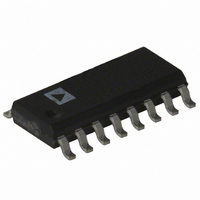
IC REG BUCK DUAL SW 1.8V 16-SOIC

ADP3156JR-1.8

Manufacturer Part Number
ADP3156JR-1.8
Description
IC REG BUCK DUAL SW 1.8V 16-SOIC
Manufacturer
Analog Devices Inc
Datasheet

Specifications of ADP3156JR-1.8

Rohs Status
RoHS non-compliant
Applications
Controller, Intel Pentium® III
Voltage - Input
3V, 5V
Number Of Outputs
2
Voltage - Output
1.8V
Operating Temperature
0°C ~ 70°C
Mounting Type
Surface Mount
Package / Case
16-SOIC (3.9mm Width)
a
Information furnished by Analog Devices is believed to be accurate and
reliable. However, no responsibility is assumed by Analog Devices for its
use, nor for any infringements of patents or other rights of third parties
which may result from its use. No license is granted by implication or
otherwise under any patent or patent rights of Analog Devices.
GENERAL DESCRIPTION
The ADP3156 is a highly efficient synchronous buck switching
regulator controller optimized for converting the 3.3 V or 5 V
main supply into lower supply voltages required on the mother-
boards of Pentium
systems. The ADP3156 uses a current mode, constant off-time
architecture to drive two external N-channel MOSFETs at a
programmable switching frequency that can be optimized for
size and efficiency. It also uses a unique supplemental regulation
technique called active voltage positioning to enhance load
transient performance. Active voltage positioning results in a
DC/DC converter that provides the best possible transient re-
sponse using the minimum number of output capacitors and
smallest footprint. Unlike voltage-mode and standard current-
mode architectures, active voltage positioning adjusts the output
voltage as a function of the load current so that it is always
optimally positioned for a system transient.
The ADP3156 provides accurate and reliable short circuit
protection and adjustable current limiting. It also includes an
integrated overvoltage crowbar function to protect the micro-
processor from destruction in case the core supply exceeds the
nominal programmed voltage by more than 15%.
Pentium is a registered trademark of Intel Corporation.
All other trademarks are the property of their respective holders.
REV. 0
FEATURES
Active Voltage Positioning with Gain and Offset
Optimal Compensation for Superior Load Transient
Fixed 1.5 V, 1.8 V and 2.5 V Output Versions
Dual N-Channel Synchronous Driver
On-Board Linear Regulator Controller
Total Output Accuracy
High Efficiency, Current-Mode Operation
Short Circuit Protection
Overvoltage Protection Crowbar Protects Loads with
Power Good Output
SO-16 Package
APPLICATIONS
Desktop Computer Supplies
ACPI-Compliant Power Systems
General Purpose DC-DC Converters
Adjustment
Response
No Additional External Components
®
III and other high performance processor
1% Over Temperature
The ADP3156 contains a linear regulator controller that is
designed to drive an external N-channel MOSFET. This linear
regulator is used to generate the auxiliary voltages (AGP, GTL,
etc.) required in most motherboard designs, and has been de-
signed to provide a high bandwidth load-transient response. A
pair of external feedback resistors sets the linear regulator out-
put voltage.
One Technology Way, P.O. Box 9106, Norwood, MA 02062-9106, U.S.A.
Tel: 781/329-4700
Fax: 781/326-8703
SD
C
1000 F
T
V
O2
Dual Power Supply Controller
V
CC
V
DRIVE1 DRIVE2 PGND
Q
T2
NONOVERLAP
IN
S
R
35k
20k
OFF-TIME
CONTROL
CROWBAR
DRIVE
FUNCTIONAL BLOCK DIAGRAM
CMPT
OFF
R1
R2
Figure 1. Typical Application
200pF
World Wide Web Site: http://www.analog.com
C
22 F
COMP
for Desktop Systems
V
SENSE–
CMPI
IN
V
REF
V
FB
CMP
AGND
SD
C
LDO
1 F
T
ADP3156
CMP
V
+15%
AGND
CC
V
SENSE+
SENSE–
CC
V
+12V
DRIVE1
DRIVE2
DELAY
REF
V
PGND
T1
g
+5% V
m
PWRGD
© Analog Devices, Inc., 1999
ADP3156
1nF
REF
V
V
ADP3156
IN
REF
REFERENCE
+5V
–5%
1.20V
+
SENSE+
C
IN
L
R
SENSE
SENSE–
R
2R
+
C
V
O
O
FB
V
LDO

Related parts for ADP3156JR-1.8

ADP3156JR-1.8 Summary of contents

Page 1

FEATURES Active Voltage Positioning with Gain and Offset Adjustment Optimal Compensation for Superior Load Transient Response Fixed 1.5 V, 1.8 V and 2.5 V Output Versions Dual N-Channel Synchronous Driver On-Board Linear Regulator Controller Total Output Accuracy 1% Over ...

Page 2

ADP3156–SPECIFICATIONS Parameter OUTPUT ACCURACY ADP3156-1.5 V ADP3156-1.8 V ADP3156-2.5 V OUTPUT VOLTAGE LINE REGULATION 2 INPUT DC SUPPLY CURRENT Normal Mode Shutdown CURRENT SENSE THRESHOLD VOLTAGE C PIN DISCHARGE CURRENT T OFF-TIME DRIVER OUTPUT TRANSITION TIME POSITIVE POWER GOOD TRIP ...

Page 3

... ORDERING GUIDE Buck Converter Model Output Voltage ADP3156JR-1.5 1.5 V ADP3156JR-1.8 1.8 V ADP3156JR-2.5 2.5 V CAUTION ESD (electrostatic discharge) sensitive device. Electrostatic charges as high as 4000 V readily accumulate on the human body and test equipment and can discharge without detection. Although the ADP3156 features proprietary ESD protection circuitry, permanent damage may occur on devices subjected to high energy electrostatic discharges ...

Page 4

ADP3156 100k ADP3156-1 SYSTEM 2 NC AGND IRL3103 6 V LDO 47pF 7 SENSE– SENSE +1. 1000 F R3 RTN 20k Figure 2. ADP3156 Typical ...

Page 5

V = 2.5V OUT V = 1.8V OUT 1.5V OUT 80 SEE FIGURE 2 75 0.5 1.5 2.5 3.5 4.5 5.5 6.5 OUTPUT CURRENT – Amps Figure 4. Efficiency vs. Output Current SEE FIGURE ...

Page 6

ADP3156 ADP3156 DRIVE1 CMP DRIVE2 1k C SENSE+ T SENSE– 4700pF AGND PGND OP27 100k 1.2V 0.1 F Figure 12. Closed-Loop Test Circuit for Accuracy THEORY OF OPERATION The ADP3156 uses a current-mode, constant-off-time control technique to ...

Page 7

During the standby operating state, the and 3.3 V power supply outputs are disabled, and only a low power 5 V rail (5VSB) is available. The circuits that must remain active in standby must be able ...

Page 8

ADP3156 The converter operates at the nominal operating frequency only at the V specified above, and at light load. At higher load OUT conditions, the operating frequency decreases due to the para- sitic voltage drops across the power devices. The ...

Page 9

A and an average short-circuit current of about 6.5 A—meaning that there is actually a small degree of short- circuit current foldback. To safely carry the maximum current, the sense resistor must have a power rating of ...

Page 10

ADP3156 Feedback Loop Compensation Design for Active Voltage Positioning Optimized compensation of the ADP3156 allows the best pos- sible containment of the peak-to-peak output voltage deviation. Any practical switching power converter is inherently limited by the inductor in its output ...

Page 11

Efficiency of the Linear Regulator The efficiency and corresponding power dissipation of the linear regulator are not determined by the ADP3156. Rather, these are a function of input and output voltage and load current. Effi- ciency is approximated by the ...

Page 12

ADP3156 9. Absolutely avoid crossing any signal lines over the switching power path loop, described below. Power Circuitry 10. The switching power path should be routed on the PCB to encompass the smallest possible area in order to minimize radiated ...

Related keywords