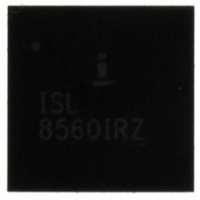
ISL8560IRZ Intersil, ISL8560IRZ Datasheet - Page 13

ISL8560IRZ
Manufacturer Part Number
ISL8560IRZ
Description
IC REG 2A DC/DC STEP-DN 20-QFN
Manufacturer
Intersil
Type
Step-Down (Buck)r
Datasheet
1.ISL8560IRZ.pdf
(17 pages)
Specifications of ISL8560IRZ
Internal Switch(s)
Yes
Synchronous Rectifier
Yes
Number Of Outputs
1
Voltage - Output
1.21 ~ 55 V
Current - Output
2A
Frequency - Switching
100kHz ~ 600kHz
Voltage - Input
9 ~ 60 V
Operating Temperature
-40°C ~ 85°C
Mounting Type
Surface Mount
Package / Case
20-VQFN Exposed Pad, 20-HVQFN, 20-SQFN, 20-DHVQFN
Power - Output
3W
Rohs Compliant
Yes
Lead Free Status / RoHS Status
Lead free / RoHS Compliant
Available stocks
Company
Part Number
Manufacturer
Quantity
Price
Company:
Part Number:
ISL8560IRZ
Manufacturer:
Intersil
Quantity:
48
Company:
Part Number:
ISL8560IRZ
Manufacturer:
Intersil
Quantity:
135
The amplitudes of the different types of voltage excursions
can be approximated by using the formulas in Equation 4:
In a typical converter design, the ESR of the output capacitor
bank dominates the transient response. The ESR and the
ESL are typically the major contributing factors in
determining the output capacitance. The number of output
capacitors can be determined by using Equation 5, which
relates the ESR and ESL of the capacitors to the transient
load step and the voltage limit (ΔVo):
If ΔV
output voltage limits, then the amount of capacitance may
need to be increased. In this situation, a trade off between
output inductance and output capacitance may be
necessary.
The ESL of the capacitors, which is an important parameter
in Equations 4 and 5, is not usually listed in databooks.
Practically, it can be approximated if an impedance vs
frequency curve is given for a specific capacitor (C):
The ESL of the capacitors becomes a concern when
designing circuits that supply power to loads with high rates
of change in the current.
Output Inductor Selection
The output inductor is selected to meet the output voltage
ripple requirements and minimize the converter’s response
time to the load transient. The inductor value determines the
converter’s ripple current and the ripple voltage is a function
of the ripple current. The ripple voltage and current are
approximated by Equation 7:
ΔV
ΔV
ΔV
I
C
Number of Caps
ESL
where f
is achieved (resonant frequency).
ΔI =
tran
where
out
ESR
SAG
HUMP
SAG
= Output Load Current Transient
= Total Output Capacitance
=
V
----------------------------------------
C 2 π
res
IN
=
=
Fs x L
(
=
and/or ΔV
ESR I
------------------------------------------------- -
C
- V
is the frequency where the lowest impedance
•
out
L
------------------------------- -
C
OUT
out
L
out
1
out
•
•
•
=
f
•
(
res
•
tran
V
•
I
-----------------------------------------------------------------------
x
ESL dI
---------------------------------
tran
V
in
I
)
tran
HUMP
out
V
2
–
V
OUT
2
V
IN
•
dt
2
out
tran
)
are found to be too large for the
ΔV
ΔV
13
ESL
+
ΔV
o
ESR I
OUT
=
ESL
•
= ΔI x ESR
tran
•
dI
---------------
dt
tran
(EQ. 4)
(EQ. 5)
(EQ. 6)
(EQ. 7)
ISL8560
Increasing the value of inductance reduces the ripple current
and voltage. However, the large inductance values reduce
the converter’s response time to a load transient. Use
approximately 30% of I
One of the parameters limiting the converter’s response to
a load transient is the time required to change the inductor
current. Given a sufficiently fast control loop design, the
ISL8560 will provide either 0% or 100% duty cycle in
response to a load transient. The response time is the time
required to slew the inductor current from an initial current
value to the transient current level. During this interval the
difference between the inductor current and the transient
current level must be supplied by the output capacitor.
Minimizing the response time can minimize the output
capacitance required.
The response time to a transient is different for the
application of load and the removal of load. Equation 8 gives
the approximate response time interval for application and
removal of a transient load:
where: I
response time to the application of load, and t
response time to the removal of load. The worst case
response time can be either at the application or removal of
load. Be sure to check both of these equations at the
minimum and maximum output levels for the worst case
response time.
Rectifier Selection
Current circulates from ground to the junction of the
MOSFET and the inductor when the high-side switch is off.
As a consequence, the polarity of the switching node is
negative with respect to ground. This voltage is
approximately -0.5V (a Schottky diode drop) during the off
time. The rectifier's rated reverse breakdown voltage must
be at least equal to the maximum input voltage, preferably
with a 20% derating factor. The power dissipation is:
Input Capacitor Selection
Use a mix of input bypass capacitors to control the voltage
overshoot across the VIN’s pin. Use small ceramic
capacitors for high frequency decoupling and bulk capacitors
to supply the current needed each time the upper MOSFET
turns on. Place the small ceramic capacitors physically close
to the VIN and PGND pins.
The important parameters for the bulk input capacitance are
the voltage rating and the RMS current rating. For reliable
P
where V
t
RISE
D
[
W
=
]
=
TRAN
D
I
V
OUT
L x I
is the voltage of the Schottky diode = 0.5V to 0.7V
IN
- V
is the transient load current step, t
TRAN
⋅
V
OUT
D
⋅
⎛
⎜
⎝
1
–
OUT
V
--------------- -
V
OUT
IN
is a good compromise.
t
FALL
⎞
⎟
⎠
=
L x I
V
OUT
TRAN
FALL
September 19, 2008
RISE
is the
(EQ. 8)
(EQ. 9)
FN9244.7
is the
Δ
I of


