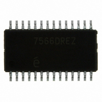
EL7566DREZ Intersil, EL7566DREZ Datasheet - Page 3

EL7566DREZ
Manufacturer Part Number
EL7566DREZ
Description
IC REG 6A DC-DC STEP DN 28HTSSOP
Manufacturer
Intersil
Type
Step-Down (Buck)r
Datasheet
1.EL7566DREZ.pdf
(14 pages)
Specifications of EL7566DREZ
Internal Switch(s)
Yes
Synchronous Rectifier
Yes
Number Of Outputs
1
Voltage - Output
0.8 ~ 6 V
Current - Output
6A
Frequency - Switching
370kHz
Voltage - Input
3 ~ 6 V
Operating Temperature
0°C ~ 85°C
Mounting Type
Surface Mount
Package / Case
28-TSSOP Exposed Pad, 28-eTSSOP, 28-HTSSOP
Lead Free Status / RoHS Status
Lead free / RoHS Compliant
Power - Output
-
Available stocks
Company
Part Number
Manufacturer
Quantity
Price
Company:
Part Number:
EL7566DREZ
Manufacturer:
INTERSIL
Quantity:
114
Part Number:
EL7566DREZ
Manufacturer:
EL
Quantity:
20 000
Company:
Part Number:
EL7566DREZ-T7
Manufacturer:
Intersil
Quantity:
4 050
Absolute Maximum Ratings
V
VX to PGND. . . . . . . . . . . . . . . . . . . . . . . . . . . . . -0.3V to V
SGND to PGND . . . . . . . . . . . . . . . . . . . . . . . . . . . . . -0.3V to +0.3V
COMP, V
SEL, PG, EN, STP, STN, C
CAUTION: Stresses above those listed in “Absolute Maximum Ratings” may cause permanent damage to the device. This is a stress only rating and operation of the
device at these or any other conditions above those indicated in the operational sections of this specification is not implied.
IMPORTANT NOTE: All parameters having Min/Max specifications are guaranteed. Typ values are for information purposes only. Unless otherwise noted, all tests are
at the specified temperature and are pulsed tests, therefore: T
DC Electrical Specifications
IN
PARAMETER
R
V
, V
I
I
R
I
V
V
OSC_CHG
VDD_OFF
V
R
V
OSC_DIS
V
REFLOAD
DSONTC2
V
V
V
DSONTC
DD_OFF
FB_LINE
I
GM
I
V
V
V
V
DD_ON
T
DD
REFTC
DSON1
PG_LO
I
LMAX
FB_TC
LEAK
I
I
PG_HI
RAMP
T
V
V
VDD
STN
STP
I
HYS
PGP
PGN
OVP
REF
F
FB
OT
FB
IN
S
REF
EA
to SGND. . . . . . . . . . . . . . . . . . . . . . . . . . . -0.3V to +6.5V
, FB, V
Input Voltage Range
Reference Accuracy
Reference Temperature Coefficient
Reference Load Regulation
Oscillator Ramp Amplitude
Oscillator Charge Current
Oscillator Discharge Current
V
V
V
V
Over-temperature Threshold
Over-temperature Hysteresis
Internal FET Leakage Current
Peak Current Limit
PMOS On Resistance
NMOS On Resistance
R
STP Pin Input Pull-down Current
STN Pin Input Pull-up Current
Positive Power Good Threshold
Negative Power Good Threshold
Power Good Drive High
Power Good Drive Low
Output Overvoltage Protection
Output Initial Accuracy
Output Line Regulation
Error Amplifier Transconductance
Output Temperature Stability
Switching Frequency
Feedback Input Pull-up Current
O
DD
DD
DD
DD
DSON
, V
Supply Current
Standby Current
for Shutdown
for Startup
TJ
, TM,
Tempco
OSC
DESCRIPTION
to SGND . . . . . -0.3V to V
3
(T
A
V
= 25°C)
DD
= V
IN
= 3.3V, T
J
= T
DD
C
IN
0 < I
0.1V < V
0.1V < V
V
EN = 0, L
V
V
With respect to target output voltage
With respect to target output voltage
I
I
V
V
V
EN = 0
I
0°C < T
= T
A
PG
PG
LOAD
EN
STP
STN
IN
CC
FB
+0.3V
+0.3V
= T
A
= 1mA
= -1mA
= 3.3V, ΔV
REF
= 0V
= 1 (L disconnected)
= 0.65V
J
= V
= V
= 0A
EL7566
= 25°C, C
A
OSC
OSC
< 50µA
X
IN
< 85°C, I
IN
= 6V (low FET), L
/2
/2
< 1.25V
< 1.25V
IN
CONDITIONS
OSC
= 10%, I
Storage Temperature . . . . . . . . . . . . . . . . . . . . . . . .-65°C to +150°C
Junction Temperature . . . . . . . . . . . . . . . . . . . . . . . . . . . . . . +125°C
Operating Ambient Temperature DRE . . . . . . . . . . . . . 0°C to +85°C
Operating Ambient Temperatute AIRE . . . . . . . . . . .-40°C to +85°C
LOAD
= 390pF, Unless Otherwise Specified
= 3A
LOAD
X
= 0V (high FET)
= 0A
1.24
0.79
MIN
300
2.4
2.6
7.8
-14
2.6
85
-1
-4
3
2
6
TYP
1.26
1.15
370
100
200
135
125
2.7
0.2
2.5
2.5
0.8
0.2
50
20
29
25
10
±1
8
1
MAX
1.28
2.65
2.95
0.81
165
440
200
1.5
0.5
0.5
10
50
14
-6
6
5
4
May 8, 2006
ppm/°C
mΩ/°C
FN7102.7
UNIT
kHz
mΩ
mΩ
mA
mA
mA
µA
°C
°C
µA
µA
µA
nA
µs
%
%
%
%
%
%
V
V
V
V
V
A
V
V
V


