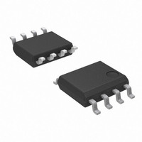
AP1513SG-13 Diodes Inc, AP1513SG-13 Datasheet - Page 7

AP1513SG-13
Manufacturer Part Number
AP1513SG-13
Description
IC CONV STEP DOWN PWM 2A 8-SOIC
Manufacturer
Diodes Inc
Type
Step-Down (Buck)r
Datasheet
1.AP1513SG-13.pdf
(9 pages)
Specifications of AP1513SG-13
Internal Switch(s)
Yes
Synchronous Rectifier
No
Number Of Outputs
1
Voltage - Output
0.8 ~ 18 V
Current - Output
2A
Frequency - Switching
300kHz
Voltage - Input
3.6 ~ 18 V
Operating Temperature
-20°C ~ 85°C
Mounting Type
Surface Mount
Package / Case
8-SOIC (3.9mm Width)
Output Voltage
+ 0.8 V to Vcc
Switching Frequency
300 KHz
Operating Temperature Range
- 40 C to + 125 C
Mounting Style
SMD/SMT
Duty Cycle (max)
0 % to 100 %
Lead Free Status / RoHS Status
Lead free / RoHS Compliant
Power - Output
-
Lead Free Status / Rohs Status
Lead free / RoHS Compliant
Other names
AP1513SG-13
AP1513SGTR
AP1513SGTR
Available stocks
Company
Part Number
Manufacturer
Quantity
Price
Company:
Part Number:
AP1513SG-13
Manufacturer:
RENESAS
Quantity:
1 100
Part Number:
AP1513SG-13
Manufacturer:
DIODES/美台
Quantity:
20 000
Functional Description
PWM Control
The AP1513 is a DC/DC converter that employs pulse width
modulation (PWM) scheme. Its pulse width varies in the range of
0% to 99%, based on the output current loading. The output
ripple voltage caused by the PWM high frequency switching can
easily be reduced through an output filter. Therefore, this
converter provides a low ripple output supply over a broad range
of input voltage & output current loading
Under Voltage Lockout
The under voltage lockout circuit of the AP1513 assures that the
high-side MOSFET driver remains in the off state whenever the
supply voltage drops below 3.3V. Normal operation resumes
once V
Current Limit Protection
The current limit threshold is set by external resistor R
connected from V
current I
at OCSET pin. When the PWM voltage is less than the voltage at
OCSET, an over-current condition is triggered.
The current limit threshold is given by the following equation:
where,
I
resistance; f
inductor value will affect the ripple current ΔI.
The above equation is recommended for input voltage range of
5V to 18V. For input voltage lower than 5V or ambient
temperature over 100°C, higher R
AP1513 Rev. 4
DS31053
PEAK
is the output peak current; R
CC
OCSET
rises above 3.5V.
S
I
PEAK
is the PWM frequency (300KHz typical). Also, the
(90μA typical) across this resistor sets the voltage
Δ
I
CC
×
PEAK
I
R
=
supply to OCSET pin. The internal sink
DS(ON)
V
IN
> I
fs
−
OUT(MAX)
×
V
=
L
OUT
I
OCSET
OCSET
DS (ON)
×
+
V
is recommended.
(Δ
×
V
OUT
IN
2
R
) I
is the MOSFET ON
OCSET
www.diodes.com
OCSET
PWM CONTROL 2A STEP-DOWN CONVERTER
7 of 9
Inductor Selection
For most designs, the operation range with inductors is from
22µH to 33µH. The inductor value can be derived from the
following equation:
Where ΔI
ripple current and small value inductors result in high ripple
current. Choose inductor ripple current approximately 15% of the
maximum load current 2A, ∆I
the inductor should be at least equal to the maximum load current
plus half the ripple current to prevent core saturation (2A+0.15A).
Input Capacitor Selection
This capacitor should be located close to the IC using short leads
and the voltage rating should be approximately 1.5 times the
maximum input voltage. The RMS current rating requirement for
the input capacitor of a buck regulator is approximately 1⁄2 the
DC load current. A low ESR input capacitor sized for maximum
RMS current must be used. A 470µF low ESR capacitor for most
applications is sufficient.
Output Capacitor Selection
The output capacitor is required to filter the output voltage and
provides regulator loop stability. The important capacitor
parameters are the 100KHz Equivalent Series Resistance (ESR),
the RMS ripples current rating, voltage rating and capacitance
value. For the output capacitor, the ESR value is the most
important parameter. The output ripple can be calculated from
the following formula.
The bulk capacitor’s ESR will determine the output ripple voltage
and the initial voltage drop after a high slew-rate transient.
An aluminum electrolytic capacitor's ESR value is related to the
capacitance and its voltage rating. In most case, higher voltage
electrolytic capacitors have lower ESR values. Most of the time,
capacitors with much higher voltage ratings may be needed to
provide the low ESR values required for low output ripple voltage.
PCB Layout Guide
If you need low T
SW pins(5& 6) and Vss pins(7& 8)on the SOP-8L package are
internally connected to die pad, The evaluation board should be
allowed for maximum copper area at output (SW) pins.
1.
2.
3.
4.
Connect FB circuits as closely as possible and keep away
from inductor flux for pure V
Connect input capacitor to Vcc and Vss pin as closely as
possible to get good power filter effect.
Connect R
possible.
Connect ground side of the input capacitor & Schottky &
output capacitor as closely as possible and use ground
plane for best performance.
L
is inductor Ripple Current. Large value inductors lower
C
OCSET
L
& T
V
=
RIPPLE
J
V
or large P
to Vcc and OCSET pin as closely as
IN
fs
−
×
V
L
=
Δ
=0.30A. The DC current rating of
OUT
ΔI
I
D
FB
L
(Power Dissipation), The dual
.
×
×
ESR
V
V
OUT
IN
©
AP1513
Diodes Incorporated
JULY 2009


