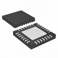
MAX5073ETI+ Maxim Integrated Products, MAX5073ETI+ Datasheet - Page 11

MAX5073ETI+
Manufacturer Part Number
MAX5073ETI+
Description
IC CONV BUCK/BOOST 28-TQFN
Manufacturer
Maxim Integrated Products
Type
Step-Down (Buck), Step-Up (Boost)r
Datasheet
1.MAX5073ETI.pdf
(25 pages)
Specifications of MAX5073ETI+
Internal Switch(s)
Yes
Synchronous Rectifier
No
Number Of Outputs
2
Voltage - Output
0.8 ~ 28 V
Current - Output
1A, 2A
Frequency - Switching
200kHz ~ 2.2MHz
Voltage - Input
4.5 ~ 23 V
Operating Temperature
-40°C ~ 85°C
Mounting Type
Surface Mount
Package / Case
28-TQFN Exposed Pad
Power - Output
2.76W
Lead Free Status / RoHS Status
Lead free / RoHS Compliant
The internal oscillator generates the 180° out-of-phase
clock signal required by each regulator. The internal
oscillator frequency is programmable from 400kHz to
4.4MHz using a single 1% resistor at R
lowing equation to calculate R
where f
and R
The two independent regulators in the MAX5073 switch
180° out-of-phase to reduce input filtering require-
ments, to reduce electromagnetic interference (EMI),
and to improve efficiency. This effectively lowers com-
ponent cost and saves board space, making the
MAX5073 ideal for cost-sensitive applications.
With dual synchronized out-of-phase operation, the
MAX5073’s high-side MOSFETs turn on 180° out-of-
phase. The instantaneous input current peaks of both
regulators do not overlap, resulting in reduced RMS rip-
ple current and input voltage ripple. This reduces the
required input capacitor ripple current rating, allows for
fewer or less expensive capacitors, and reduces
shielding requirements for EMI. The out-of-phase wave-
forms in the Typical Operating Characteristics demon-
strate synchronized 180° out-of-phase operation.
The main oscillator can be synchronized to the system
clock by applying an external clock (f
The f
ating frequency of an individual converter. Use a TTL
logic signal for the external clock with at least a 100ns
pulse width. R
synchronization. Program the internal oscillator fre-
quency so 0.2f
edge of f
internal MOSFET (see Figure 3).
where f
and R
Two MAX5073s can be connected in the master-slave
configuration for four ripple-phase operation. The
MAX5073 provides a clock output (CLKOUT) that is 45°
phase-shifted with respect to the internal switch turn-on
edge. Feed the CLKOUT of the master to the SYNC
Internal Oscillator/Out-of-Phase Operation
2.2MHz, Dual-Output Buck or Boost Converter
SYNC
OSC
OSC
OSC
OSC
SYNC
in ohms.
in ohms, f
frequency must be twice the required oper-
is the internal oscillator frequency in hertz
is the internal oscillator frequency in hertz
OSC
synchronizes the turn-on edge of the
SYNC
______________________________________________________________________________________
R
R
is still required when using external
OSC
OSC
OSC
< f
Synchronization (SYNC)/
=
Clock Output (CLKOUT)
= 2 x f
=
OSC
25
25
f
OSC
f
OSC
×
OSC
×
< 1.2f
SW
10
10
:
.
9
9
SYNC
OSC
SYNC
. Use the fol-
. The rising
with Internal Power MOSFETs
) at SYNC.
input of the slave. The effective input ripple switching
frequency shall be four times the individual converter’s
switching frequency. When driving the master convert-
er using external clock at SYNC, set the clock duty
cycle to 50% for a 90° phase-shifted operation.
All internal control circuitry operates from an internally
regulated nominal voltage of 5.2V (VL). At higher input
voltages (V+) of 5.5V to 23V, VL is regulated to 5.2V.
At 5.5V or below, the internal linear regulator operates
in dropout mode, where VL follows V+. Depending on
the load on VL, the dropout voltage can be high
enough to reduce VL below the undervoltage lockout
(UVLO) threshold.
For input voltages of less than 5.5V, connect V+ and VL
together. The load on VL is proportional to the switch-
ing frequency of converter 1 and converter 2. See the
Dropout Voltage vs. Switching Frequency graph in the
Typical Operating Characteristics. For input voltage
ranges higher than 5.5V, use the internal regulator.
Bypass V+ to SGND with a low-ESR, 0.1µF or greater
ceramic capacitor placed close to the MAX5073. Current
spikes from VL may disturb internal circuitry powered by
VL. Bypass VL with a low-ESR, ceramic 0.1µF capacitor
to PGND and 4.7µF capacitor to SGND.
The MAX5073 includes an undervoltage lockout with
hysteresis and a power-on-reset circuit for converter
turn-on and monotonic rise of the output voltage. The
rising UVLO threshold is internally set to 4.3V with a
175mV hysteresis. Hysteresis at UVLO eliminates “chat-
tering” during startup. When VL drops below UVLO, the
internal switches are turned off.
Digital soft-start is provided internally to reduce input
surge currents and glitches at the input during turn-on.
When UVLO is cleared and EN_ is high, digital soft-
start slowly ramps up the internal reference voltage in
64 steps. The total soft-start period is 2048 switching
cycles of the internal oscillator.
To calculate the soft-start period, use the following
equation:
where f
which is twice the switching frequency of each converter.
OSC
Input Voltage (V+)/Internal Linear
is the internal oscillator frequency in hertz,
Undervoltage Lockout/Soft-Start
t
SS
=
2048
f
OSC
Regulator (VL)
11


