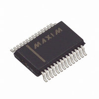
MAX1634CAI+ Maxim Integrated Products, MAX1634CAI+ Datasheet - Page 22

MAX1634CAI+
Manufacturer Part Number
MAX1634CAI+
Description
IC PS CTRLR NOTEBOOK 28-SSOP
Manufacturer
Maxim Integrated Products
Type
Step-Down (Buck)r
Datasheet
1.MAX1634CAI.pdf
(29 pages)
Specifications of MAX1634CAI+
Internal Switch(s)
No
Synchronous Rectifier
Yes
Number Of Outputs
2
Voltage - Output
3.3V, 5V, Adj
Current - Output
4A
Frequency - Switching
200kHz, 300kHz
Voltage - Input
4.2 ~ 30 V
Operating Temperature
0°C ~ 70°C
Mounting Type
Surface Mount
Package / Case
28-SSOP
Power - Output
762mW
Output Voltage
2.5 V to 5.5 V, 3.3 V, 5 V
Input Voltage
4.2 V to 30 V
Mounting Style
SMD/SMT
Maximum Operating Temperature
+ 70 C
Minimum Operating Temperature
0 C
Lead Free Status / RoHS Status
Lead free / RoHS Compliant
________________Applications Information
The major efficiency-loss mechanisms under loads are,
in the usual order of importance:
• P(I
• P(tran) = transition losses
• P(gate) = gate-charge losses
• P(diode) = diode-conduction losses
• P(cap) = capacitor ESR losses
• P(IC) = losses due to the IC’s operating supply
Inductor core losses are fairly low at heavy loads
because the inductor’s AC current component is small.
Therefore, they aren’t accounted for in this analysis.
Ferrite cores are preferred, especially at 300kHz, but
powdered cores, such as Kool-Mu, can work well.
Multi-Output, Low-Noise Power-Supply
Controllers for Notebook Computers
Table 5. Low-Voltage Troubleshooting Chart
22
supply current
Sag or droop in V
step-load change
Dropout voltage is too high
(V
decreases)
Unstable—jitters between
different duty factors and
frequencies
Secondary output won’t
support a load
Poor efficiency
Won’t start under load or
quits before battery is
completely dead
Efficiency = P
P
P = (I R) = (I
TOTAL
OUT
2
______________________________________________________________________________________
R) = I
Heavy-Load Efficiency Considerations
2
follows V
SYMPTOM
= P(I R) + P(tran) + P(gate) +
2
R losses
= P
P(diode) + P(cap) + P(IC)
LOAD
2
OUT
OUT
IN
OUT
as V
) x (R
2
/ (P
/ P x 100%
under
IN
IN
OUT
DC
+ P
+ R
Low V
differential, <1.5V
Low V
differential, <1V
Low V
differential, <0.5V
Low V
differential,
V
Low input voltage, <5V
Low input voltage, <4.5V
TOTAL
IN
DS(ON)
< 1.3 x V
CONDITION
IN
IN
IN
IN
) x 100%
-V
-V
-V
-V
OUT
OUT
OUT
OUT
+ R
OUT
SENSE
(main)
)
Limited inductor-current
slew rate per cycle.
Maximum duty-cycle limits
exceeded.
Normal function of internal
low-dropout circuitry.
Not enough duty cycle left
to initiate forward-mode
operation. Small AC current
in primary can’t store ener-
gy for flyback operation.
VL linear regulator is going
into dropout and isn’t provid-
ing good gate-drive levels.
VL output is so low that it
hits the VL UVLO threshold.
where R
the MOSFET on-resistance, and R
sense resistor value. The R
cal MOSFETs for the high-side and low-side switches,
because they time-share the inductor current. If the
MOSFETs aren’t identical, their losses can be estimat-
ed by averaging the losses according to duty factor.
where C
high-side MOSFET (a data-sheet parameter), I
DH gate-driver peak output current (1.5A typical), and
20ns is the rise/fall time of the DH driver (20ns typical).
where VL is the internal-logic-supply voltage (+5V), and qG
is the sum of the gate-charge values for low-side and high-
side switches. For matched MOSFETs, qG is twice the
data-sheet value of an individual MOSFET. If V
less than 4.5V, replace VL in this equation with V
this case, efficiency can be improved by connecting VL to
an efficient 5V source, such as the system +5V supply.
ROOT CAUSE
PD(tran) = transition loss = V x I
DC
RSS
P(diode) = diode - conduction losses
is the DC resistance of the coil, R
is the reverse transfer capacitance of the
[
(V x C
IN
P(gate) = qG x f x VL
= I
RSS
LOAD
Increase bulk output capacitance
per formula (see Low-Voltage
Operation section). Reduce inductor
value.
Reduce operation to 200kHz.
Reduce MOSFET on-resistance and
coil DCR.
Increase the minimum input voltage
or ignore.
Reduce operation to 200kHz.
Reduce secondary impedances;
use a Schottky diode, if possible.
Stack secondary winding on the
main output.
Use a small 20mA Schottky diode
for boost diode D2. Supply VL from
an external source.
Supply VL from an external source
other than V
+5V supply.
/ I
GATE
DS(ON)
x V
FWD
IN
) + 20ns
SOLUTION
IN
SENSE
term assumes identi-
, such as the system
LOAD
x t x f
D
]
x f x
is the current-
OUT
GATE
3
2
DS(ON)
BATT
x
is set to
is the
. In
is


