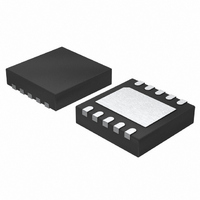
LT3463EDD#TRPBF Linear Technology, LT3463EDD#TRPBF Datasheet - Page 3

LT3463EDD#TRPBF
Manufacturer Part Number
LT3463EDD#TRPBF
Description
IC CONV DC/DC DUAL MICRPWR 10DFN
Manufacturer
Linear Technology
Type
Invertingr
Datasheet
1.LT3463AEDDPBF.pdf
(8 pages)
Specifications of LT3463EDD#TRPBF
Internal Switch(s)
Yes
Synchronous Rectifier
No
Number Of Outputs
2
Voltage - Output
1.25 ~ 40 V
Current - Output
250mA
Voltage - Input
2.4 ~ 15 V
Operating Temperature
-40°C ~ 85°C
Mounting Type
Surface Mount
Package / Case
10-DFN
Lead Free Status / RoHS Status
Lead free / RoHS Compliant
Power - Output
-
Frequency - Switching
-
Available stocks
Company
Part Number
Manufacturer
Quantity
Price
PI FU CTIO S
V
cathode of an internal Schottky diode whose anode is
connected to the SW1 pin.
SW1 (Pin 2): Switch Pin for Switcher 1. This is the
collector of the internal NPN switch. Minimize the metal
trace area connected to this pin to minimize EMI.
V
capacitor as close to the device as possible.
SW2 (Pin 4): Switch Pin for Switcher 2. This is the
collector of the internal NPN switch. Minimize the metal
trace area connected to this pin to minimize EMI.
TYPICAL PERFOR A CE CHARACTERISTICS
OUT1
IN
900
800
700
600
500
400
300
200
100
400
350
300
250
200
150
100
50
U
0
0
–50
(Pin 3): Input Supply Pin. Bypass this pin with a
–50
Switch Off Time
V
CESAT
(Pin 1): Output Voltage Switcher 1. This is the
I
I
DIODE
SWITCH
–25
–25
U
= 150mA
and V
= 150mA
0
0
TEMPERATURE ( C)
TEMPERATURE ( C)
DIODE
25
25
FOR BOTH SWITCHERS
U
Voltage
50
50
75
75
W
100
100
3463 G01
3463 G04
U
125
125
1.27
1.26
1.25
1.24
1.23
1.22
450
400
350
300
250
200
150
100
50
0
–50
–50
V
Switch Current Limit
REF
–25
–25
and V
0
0
TEMPERATURE ( C)
TEMPERATURE ( C)
LT3463 SW1, SW2
FB1
LT3463A SW2
LT3463A SW1
25
25
Voltage
D2 (Pin 5): Diode for Switcher 2. This is the anode of an
internal Schottky diode whose cathode connected to the
GND pin.
FB2 (Pin 6): Feedback Pin for Switcher 2. Set the output
voltage by selecting values for R3 and R4.
V
used along with FB2 to set the negative output voltage for
Switcher 2.
SHDN2 (Pin 8): Shutdown Pin for Switcher 2. Pull this pin
above 1.5V to enable Switcher 2. Pull below 0.3V to turn
it off. Do not leave this pin floating.
50
REF
50
V
FB1
(Pin 7): Voltage Reference Pin (1.25V). This pin is
75
75
V
REF
100
100
3463 G02
3463 G05
125
125
10
60
50
40
30
20
10
8
6
4
2
0
0
LT3463/LT3463A
–50
–50
V
Quiescent Current
FB2
NOT SWITCHING
V
V
FB1
FB2
–25
–25
Voltage
= 1.3V
= –0.1V
0
0
TEMPERATURE ( C)
TEMPERATURE ( C)
25
25
50
50
75
75
100
100
3463 G03
3463 G06
3
3463f
125
125


