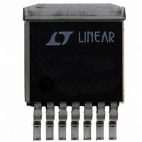
LT1374CR-5 Linear Technology, LT1374CR-5 Datasheet - Page 25

LT1374CR-5
Manufacturer Part Number
LT1374CR-5
Description
IC SW REG 4.5A 5V STEP-DWN 7-DD
Manufacturer
Linear Technology
Type
Step-Down (Buck)r
Datasheet
1.LT1374CFEPBF.pdf
(32 pages)
Specifications of LT1374CR-5
Internal Switch(s)
Yes
Synchronous Rectifier
No
Number Of Outputs
1
Voltage - Output
5V
Current - Output
4.5A
Frequency - Switching
500kHz
Voltage - Input
5 ~ 25 V
Operating Temperature
0°C ~ 125°C
Mounting Type
Surface Mount
Package / Case
D²Pak, TO-263 (7 leads + tab)
Lead Free Status / RoHS Status
Contains lead / RoHS non-compliant
Power - Output
-
Available stocks
Company
Part Number
Manufacturer
Quantity
Price
Company:
Part Number:
LT1374CR-5
Manufacturer:
Linear Technology
Quantity:
135
Company:
Part Number:
LT1374CR-5
Manufacturer:
DSP
Quantity:
2 000
Company:
Part Number:
LT1374CR-5#PBF
Manufacturer:
LT
Quantity:
1 900
Part Number:
LT1374CR-5#PBF
Manufacturer:
LINEAR/凌特
Quantity:
20 000
Company:
Part Number:
LT1374CR-5#TRPBF
Manufacturer:
LT
Quantity:
1 900
Company:
Part Number:
LT1374CR-5.0
Manufacturer:
LT
Quantity:
1
APPLICATIONS
likely to be changed in production is the output capacitor,
because that is the component most likely to have manu-
facturer variations (in ESR) large enough to cause prob-
lems. It would be a wise move to lock down the sources of
the output capacitor in production.
A possible exception to the “clean response” rule is at very
light loads, as evidenced in Figure 14 with I
Switching regulators tend to have dramatic shifts in loop
response at very light loads, mostly because the inductor
current becomes discontinuous. One common result is very
slow but stable characteristics. A second possibility is low
phase margin, as evidenced by ringing at the output with
transients. The good news is that the low phase margin at
light loads is not particularly sensitive to component varia-
tion, so if it looks reasonable under a transient test, it will
probably not be a problem in production. Note that fre-
quency of the light load ringing may vary with component
tolerance but phase margin generally hangs in there.
POSITIVE-TO-NEGATIVE CONVERTER
The circuit in Figure 15 is a classic positive-to-negative
topology using a grounded inductor. It differs from the
standard approach in the way the IC chip derives its
feedback signal, however, because the LT1374 accepts
only positive feedback signals, the ground pin must be tied
to the regulated negative output. A resistor divider to
ground or, in this case, the sense pin, then provides the
proper feedback voltage for the chip.
5.5V TO
** MAXIMUM LOAD CURRENT DEPENDS ON MINIMUM INPUT VOLTAGE
INPUT
* INCREASE L1 TO 10µH OR 20µH FOR HIGHER CURRENT APPLICATIONS.
10µF TO
SEE APPLICATIONS INFORMATION
AND INDUCTOR SIZE. SEE APPLICATIONS INFORMATION
20V
50µF
C3
+
Figure 15. Positive-to-Negative Converter
V
IN
GND
LT1374-5
BOOST
U
V
C
SENSE
R
INFORMATION
V
C
C
SW
U
C
D2
MBRS330T3
C2
0.27µF
W
CMDSH-3
D3
5µH
L1*
D1
LOAD
+
U
C1
100µF
10V TANT
× 2
= 50mA.
OUTPUT**
–5V, 1.8A
1374 F15
Inverting regulators differ from buck regulators in the
basic switching network. Current is delivered to the output
as square waves with a peak-to-peak amplitude much
greater than load current . This means that maximum load
current will be significantly less than the LT1374’s 4.5A
maximum switch current, even with large inductor values .
The buck converter in comparison, delivers current to the
output as a triangular wave superimposed on a DC level
equal to load current, and load current can approach 4.5A
with large inductors. Output ripple voltage for the positive-
to-negative converter will be much higher than a buck
converter. Ripple current in the output capacitor will also
be much higher. The following equations can be used to
calculate operating conditions for the positive-to-negative
converter.
Maximum load current:
I
V
V
V
0.35 = Switch voltage drop at 4.5A
Example: with V
V
not take into account that maximum rated switch current
(I
above 50%. If duty cycle is expected to exceed 50% (input
voltage less than output voltage), use the actual I
from the Electrical Characteristics table.
Operating duty cycle:
(This formula uses an average value for switch loss, so it
may be several percent in error.)
P
IN
OUT
F
F
P
= Maximum rated switch current
= 0.5V, I
) on the LT1374 is reduced slightly for duty cycles
= Catch diode forward voltage
= Minimum input voltage
= Output voltage
P
= 4.5A: I
IN(MIN)
MAX
= 2A. Note that this equation does
= 5.5V, V
OUT
= 5V, L = 10µH,
LT1374
25
P
value
1374fd


