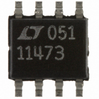
LTC1147CS8-3.3 Linear Technology, LTC1147CS8-3.3 Datasheet - Page 13

LTC1147CS8-3.3
Manufacturer Part Number
LTC1147CS8-3.3
Description
IC SW REG STEP-DOWN 3.3V 8-SOIC
Manufacturer
Linear Technology
Type
Step-Down (Buck)r
Datasheet
1.LTC1147CN8-3.3.pdf
(16 pages)
Specifications of LTC1147CS8-3.3
Internal Switch(s)
No
Synchronous Rectifier
No
Number Of Outputs
1
Voltage - Output
3.3V
Current - Output
50mA
Frequency - Switching
400kHz
Voltage - Input
3.5 ~ 14 V
Operating Temperature
0°C ~ 70°C
Mounting Type
Surface Mount
Package / Case
8-SOIC (3.9mm Width)
Lead Free Status / RoHS Status
Contains lead / RoHS non-compliant
Power - Output
-
Available stocks
Company
Part Number
Manufacturer
Quantity
Price
Company:
Part Number:
LTC1147CS8-3.3
Manufacturer:
LT
Quantity:
10 000
Part Number:
LTC1147CS8-3.3
Manufacturer:
LINEAR/凌特
Quantity:
20 000
Company:
Part Number:
LTC1147CS8-3.3#PBF
Manufacturer:
LTC
Quantity:
535
Company:
Part Number:
LTC1147CS8-3.3#TRPBF
Manufacturer:
LINEAR
Quantity:
12 411
Company:
Part Number:
LTC1147CS8-3.3TR
Manufacturer:
PHILIPS
Quantity:
2 813
APPLICATIO S I FOR ATIO
Board Layout Checklist
When laying out the printed circuit board, the following
checklist should be used to ensure proper operation of the
LTC1147 series. These items are also illustrated graphi-
cally in the layout diagram of Figure 7. Check the following
in your layout:
1. Are the signal and power grounds segregated? The
2. Does the LTC1147 SENSE
LTC1147 ground (Pin 7) must return separately to a)
the power and b) signal grounds. The power ground
(a) returns to the source anode of the Schottky diode
and (–) plate of C
as short as possible. The signal ground (b) connects
to the (–) plate of C
close to R
V
+
–
IN
BOLD LINES INDICATE HIGH CURRENT PATHS
SENSE
390pF
U
and the (+) plate of C
IN
1k
, which should have lead lengths
OUT
3300pF
U
.
–
Figure 7. LTC1147 Layout Diagram (See Board Layout Checklist)
(Pin 4) connect to a point
1
2
3
4
V
C
I
SENSE
TH
IN
T
W
LTC1147-3.3
(LTC1147L)
LTC1147-5
–
+
+
1 F
OUT
C
SENSE
PDRIVE
IN
?
1000pF
SHDN
(V
GND
U
FB
+
)
8
7
6
5
P-CH
SHUTDOWN
3. Are the SENSE
4. Does the (+) plate of C
5. Is the input decoupling capacitor (0.1 F/1 F) con-
6. On fixed output versions, is the SHDN (Pin 6) actively
For additional High Efficiency application circuits see Application Note 54.
100pF
minimum PC trace spacing? The 1000pF capacitor
between Pins 4 and 5 should be as close as possible to
the LTC1147.
P-channel MOSFET as closely as possible? This capaci-
tor provides the AC current to the P-channel MOSFET.
nected closely between V
This capacitor carries the MOSFET driver peak currents.
pulled to ground during normal operation? The SHDN
pin is high impedance and must not be allowed to float.
D1
R1
L
LTC1147-5/LTC1147L
–
R2
and SENSE
R
SENSE
IN
IN
connect to the source of the
(Pin 1) and ground (Pin 7)?
LTC1147 • F07
+
OUTPUT DIVIDER
REQUIRED WITH
ADJUSTABLE
VERSION ONLY
leads routed together with
LTC1147-3.3
+
C
OUT
V
OUT
+
–
sn1147 1147fds
13


