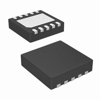
ISL97656IRTZ-T Intersil, ISL97656IRTZ-T Datasheet - Page 6

ISL97656IRTZ-T
Manufacturer Part Number
ISL97656IRTZ-T
Description
IC VREG STEP-UP HF/HE 10-TDFN
Manufacturer
Intersil
Type
Step-Up (Boost)r
Datasheet
1.ISL97656IRTZ-TK.pdf
(8 pages)
Specifications of ISL97656IRTZ-T
Internal Switch(s)
Yes
Synchronous Rectifier
No
Number Of Outputs
1
Voltage - Output
5 ~ 25 V
Current - Output
1A
Frequency - Switching
640kHz, 1.2MHz
Voltage - Input
2.3 ~ 6 V
Operating Temperature
-40°C ~ 85°C
Mounting Type
Surface Mount
Package / Case
10-TDFN Exposed Pad
Lead Free Status / RoHS Status
Lead free / RoHS Compliant
Power - Output
-
Available stocks
Company
Part Number
Manufacturer
Quantity
Price
Part Number:
ISL97656IRTZ-TK
Manufacturer:
INTERSIL
Quantity:
20 000
Output Voltage
An external feedback resistor divider is required to divide the
output voltage down to the nominal 1.24V reference voltage.
The current drawn by the resistor network should be limited
to maintain the overall converter efficiency. The maximum
value of the resistor network is limited by the feedback input
bias current and the potential for noise being coupled into
the feedback pin. A resistor network less than 100k is
recommended. The boost converter output voltage is
determined by the relationship as shown in Equation 4. The
nominal VFB voltage is 1.24V..
V
Inductor Selection
The inductor selection determines the output ripple voltage,
transient response, output current capability, and efficiency.
Its selection depends on the input voltage, output voltage,
switching frequency, and maximum output current. For most
applications, the inductance should be in the range of 2µH to
33µH. The inductor maximum DC current specification must
be greater than the peak inductor current required by the
regulator. The peak inductor current can be calculated using
Equation 5::
Output Capacitor
Low ESR capacitors should be used to minimized the output
voltage ripple. Multilayer ceramic capacitors (X5R and X7R)
are preferred for the output capacitors because of their lower
ESR and small packages. Tantalum capacitors with higher
ESR can also be used. The output ripple can be calculated
using Equation 6:
For noise sensitive application, a 0.1µF placed in parallel
with the larger output capacitor is recommended to reduce
the switching noise coupled from the LX switching node.
I
ΔV
L PEAK
OUT
FIGURE 10. BOOST CONVERTER - CYCLE 2, POWER
(
O
V
=
IN
=
------------------------ -
f
I
)
SW
C
V
OUT
=
IN
FB
I
----------------------------------- -
×
OUT
×
×
C
SWITCH OPEN
⎛
⎜
⎝
D
O
1
V
+
+
×
IN
I
V
R
------ -
R
OUT
L
OUT
1
2
ISL97656
⎞
⎟
⎠
ΔI
L2
×
+
ESR
1 2 ⁄
ΔT
2
6
×
I
V
---------------------------------------------------- -
L
L
D
IN
×
V
×
ΔV
OUT
(
V
O
OUT
×
C
FREQ
OUT
–
V
IN
)
V
(EQ. 5)
(EQ. 4)
(EQ. 6)
OUT
ISL97656
Schottky Diode
In selecting the Schottky diode, the reverse break down
voltage, forward current and forward voltage drop must be
considered for optimum converter performance. The diode
must be rated to handle 4.0A, the current limit of the
ISL97656. The breakdown voltage must exceed the
maximum output voltage. Low forward voltage drop, low
leakage current, and fast reverse recovery will help the
converter to achieve the maximum efficiency.
Input Capacitor
The value of the input capacitor depends the input and
output voltages, the maximum output current, the inductor
value and the noise allowed to put back on the input line. For
most applications, a minimum 10µF is required. For
applications that run close to the maximum output current
limit, input capacitor in the range of 22µF to 47µF is
recommended.
The ISL97656 is powered from the VIN. A High frequency
0.1µF bypass capacitor is recommended to be close to the VIN
pin to reduce supply line noise and ensure stable operation.
Loop Compensation
The ISL97656 incorporates a transconductance amplifier in
its feedback path to allow the user some adjustment on the
transient response and better regulation. The ISL97656
uses current mode control architecture which has a fast
current sense loop and a slow voltage feedback loop. The
fast current feedback loop does not require any
compensation. The slow voltage loop must be compensated
for stable operation. The compensation network is a series
RC network from COMP pin to ground. The resistor sets the
high frequency integrator gain for fast transient response
and the capacitor sets the integrator zero to ensure loop
stability. For most applications, the compensation resistor in
the range of 0k to 2.0k and the compensation capacitor in
the range of 3nF to 10nF.
Soft-Start
The soft-start is provided by an internal 4.5µA current source
charges the external C
limited by the voltage on the capacitor. This in turn controls
the rising rate of the output voltage. The regulator goes
through the start-up sequence as well after the EN pin is
pulled to HI.
Frequency Selection
The ISL97656 switching frequency can be user selected to
operate at either constant 640kHz or 1.25MHz. Connecting
FREQ pin to ground sets the PWM switching frequency to
640kHz. When connecting FREQ high or IN, the switching
frequency is set to 1.2MHz.
Shutdown Control
When the EN pin is pulled down, the ISL97656 is shutdown
reducing the supply current to <1µA.
SS
, the peak MOSFET current is
April 2, 2010
FN6439.4


