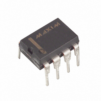
MAX680CPA Maxim Integrated Products, MAX680CPA Datasheet - Page 7

MAX680CPA
Manufacturer Part Number
MAX680CPA
Description
IC VOLT CONV CMOS HI-EFF 8-DIP
Manufacturer
Maxim Integrated Products
Type
Step-Up (Boost), Switched Capacitor (Charge Pump), Invertingr
Datasheet
1.MAX680CPA.pdf
(8 pages)
Specifications of MAX680CPA
Internal Switch(s)
Yes
Synchronous Rectifier
No
Number Of Outputs
2
Voltage - Output
±4 ~ ±12 V
Current - Output
10mA
Frequency - Switching
8kHz
Voltage - Input
2 ~ 6 V
Operating Temperature
0°C ~ 70°C
Mounting Type
Through Hole
Package / Case
8-DIP (0.300", 7.62mm)
Power - Output
727mW
Function
Inverting, Step Up
Output Voltage
+/- 10 V
Output Current
10 mA
Maximum Operating Temperature
+ 70 C
Minimum Operating Temperature
0 C
Mounting Style
Through Hole
Lead Free Status / RoHS Status
Contains lead / RoHS non-compliant
Available stocks
Company
Part Number
Manufacturer
Quantity
Price
Company:
Part Number:
MAX680CPA
Manufacturer:
MAXIM
Quantity:
5 510
Part Number:
MAX680CPA
Manufacturer:
MAXIM/美信
Quantity:
20 000
Paralleling multiple MAX680/MAX681s reduces the out-
put resistance of both the positive and negative con-
verters. The effective output resistance is the output
resistance of a single device divided by the number of
devices. As Figure 4 shows, each MAX680 requires
separate pump capacitors C1 and C2, but all can
share a single set of reservoir capacitors.
Figure 5 shows a complete ±5V power supply using one
3V battery. The MAX680/MAX681 provide +6V at V+,
which is regulated to +5V by the MAX666, and -6V,
which is regulated to -5V by the MAX664. The MAX666
and MAX664 are pretrimmed at wafer sort and require
Figure 5. Regulated +5V and -5V from a Single Battery
6V TO 3V
100 F
100 F
±5V Regulated Supplies from
_______________________________________________________________________________________
C1+
C1-
C2+
C2-
a Single 3V Battery
Paralleling Devices
MAX680
GND
V
CC
+5V to ±10V Voltage Converters
V+
V-
100 F
100 F
2M
1.2M
no external setting resistors, minimizing part count. The
combined quiescent current of the MAX680/MAX681,
MAX663, and MAX664 is less than 500µA, while the out-
put current capability is 5mA. The MAX680/MAX681
input can vary from 3V to 6V without affecting regulation
appreciably. With higher input voltage, more current can
be drawn from the MAX680/MAX681 outputs. With 5V at
V
simultaneously. Assuming 150Ω source resistance for
both converters, with (I
charge pump will droop 3V, providing +7V for the nega-
tive charge pump. The negative charge pump will droop
another 1.5V due to its 10mA load, leaving -5.5V at V-
sufficient to maintain regulation for the MAX664 at this
current.
0.1 F
0.1 F
+12V TO +6V
-12V TO -6V
CC
, 10mA can be drawn from both regulated outputs
LBI
VIN
V
GND
GND
IN
MAX666
MAX664
LBO
SDN
SDN
SENSE
VOUT1
VOUT2
SENSE
VOUT
VSET
V
SET
L +
+ I
10 F
10 F
L -
) = 20mA, the positive
LOW-BATTERY
WARNING AT 3.5V
GND
+5V
-5V
7


