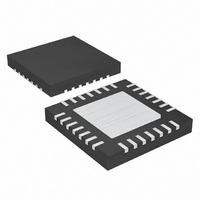
MAX5073ATI+T Maxim Integrated Products, MAX5073ATI+T Datasheet - Page 16

MAX5073ATI+T
Manufacturer Part Number
MAX5073ATI+T
Description
IC CONV BUCK/BOOST 28-TQFN
Manufacturer
Maxim Integrated Products
Type
Step-Down (Buck), Step-Up (Boost)r
Datasheet
1.MAX5073ETI.pdf
(25 pages)
Specifications of MAX5073ATI+T
Internal Switch(s)
Yes
Synchronous Rectifier
No
Number Of Outputs
2
Voltage - Output
0.8 ~ 28 V
Current - Output
1A, 2A
Frequency - Switching
200kHz ~ 2.2MHz
Voltage - Input
4.5 ~ 23 V
Operating Temperature
-40°C ~ 85°C
Mounting Type
Surface Mount
Package / Case
28-TQFN Exposed Pad
Power - Output
2.76W
Lead Free Status / RoHS Status
Lead free / RoHS Compliant
Three key inductor parameters must be specified for
operation with the MAX5073: inductance value (L), peak
inductor current (I
(I
operating frequency, input-to-output voltage differential
and the peak-to-peak inductor current (∆I
allows for a lower inductor value while a lower ∆I
requires a higher inductor value. A lower inductor value
minimizes size and cost, improves large-signal transient
response, but reduces efficiency due to higher peak cur-
rents and higher peak-to-peak output ripple voltage for
the same output capacitor. On the other hand, higher
inductance increases efficiency by reducing the ripple
current. However, resistive losses due to extra wire turns
can exceed the benefit gained from lower ripple current
levels, especially when the inductance is increased with-
out also allowing for larger inductor dimensions. A good
compromise is to choose ∆I
current. To calculate the inductance use the following
equation:
where V
cy is optimum for typical conditions). The switching fre-
quency is set by R
Frequency section). The peak-to-peak inductor current,
which reflects the peak-to-peak output ripple, is worse
at the maximum input voltage. See the Output Capacitor
Selection section to verify that the worst-case output rip-
ple is acceptable. The inductor saturating current is also
important to avoid runaway current during output over-
load and continuous short circuit. Select the I
higher than the maximum peak current limits of 4.5A
and 2.2A for converter 1 and converter 2.
The discontinuous input current waveform of the buck
converter causes large ripple currents at the input. The
switching frequency, peak inductor current, and the
allowable peak-to-peak voltage ripple dictate the input
capacitance requirement. Increasing the switching fre-
quency or the inductor value lowers the peak to aver-
age current ratio, yielding a lower input capacitance
requirement. Note that two converters of MAX5073 run
180° out-of-phase, thereby effectively doubling the
switching frequency at the input.
2.2MHz, Dual-Output Buck or Boost Converter
with Internal Power MOSFETs
16
SAT
______________________________________________________________________________________
). The minimum required inductance is a function of
IN
and V
L
OUT
=
L
V
V
OSC
), and inductor saturation current
OUT IN
IN
are typical values (so that efficien-
×
(
(see the Setting the Switching
V
f
L
SW
equal to 30% of the full load
−
V
× ∆
OUT
I
L
Inductor Selection
)
Input Capacitors
L
). Higher ∆I
SAT
to be
L
L
The input ripple waveform would be unsymmetrical due
to the difference in load current and duty cycle
between converter 1 and converter 2. The input ripple
is comprised of ∆V
charge) and ∆V
tor). A higher load converter dictates the ESR
requirement, while the capacitance requirement is a
function of the loading mismatch between the two con-
verters. The worst-case mismatch is when one converter
is at full load while the other is at no load or in shutdown.
Use low-ESR ceramic capacitors with high ripple-cur-
rent capability at the input. Assume the contribution
from the ESR and capacitor discharge equal to 50%.
Calculate the input capacitance and ESR required for a
specified ripple using the following equations:
where
and
where
where I
converter 1 or converter 2, and D is the duty cycle for
that converter. f
converter. For example, at V
I
capacitance are calculated for a peak-to-peak input
ripple of 100mV or less, yielding an ESR and capaci-
tance value of 20mΩ and 6.8µF for 1.25MHz frequency.
Use a 100µF capacitor at low input voltages to avoid
possible undershoot below the undervoltage lockout
threshold during power-on and transient loading.
OUT
= 2A, and with L = 3.3µH, the ESR and input
OUT
∆I
is the maximum output current from either
L
ESR
C
ESR
=
SW
IN
(
V
IN
=
IN
is the frequency of each individual
(caused by the ESR of the capaci-
Q
V
I
D
=
OUT
IN
−
(caused by the capacitor dis-
∆
=
⎛
⎜
⎝
V
I
V
×
OUT
OUT
V
Q
OUT
V
∆
×
f
IN
SW
V
×
IN
)
ESR
D
+
×
(
f
= 12V, V
1
SW
∆
×
2
−
I
L
V
D
OUT
L
⎞
⎟
⎠
)
OUT
= 3.3V at


