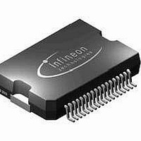
TLE6361G Infineon Technologies, TLE6361G Datasheet - Page 16

TLE6361G
Manufacturer Part Number
TLE6361G
Description
IC PS SYSTEM MULTI VOLT PDSO-36
Manufacturer
Infineon Technologies
Type
Step-Down (Buck)r
Datasheet
1.TLE6361G.pdf
(57 pages)
Specifications of TLE6361G
Internal Switch(s)
Yes
Synchronous Rectifier
No
Number Of Outputs
4
Voltage - Output
5.4 ~ 6.05 V
Current - Output
1.5A
Frequency - Switching
370kHz
Voltage - Input
5.5 ~ 60 V
Operating Temperature
-40°C ~ 150°C
Mounting Type
Surface Mount
Package / Case
DSO-36
Output Voltage
5.5 V
Output Current
1.5 A
Input Voltage Max
60 V
Maximum Operating Temperature
+ 150 C
Minimum Operating Temperature
- 40 C
Mounting Style
SMD/SMT
Operating Temperature Range
- 40 C to + 150 C
Output Voltage Tolerance
+/- 10 %
Lead Free Status / RoHS Status
Contains lead / RoHS non-compliant
Power - Output
-
Lead Free Status / Rohs Status
Lead free / RoHS Compliant
Other names
SP000013297
TLE6361GNT
TLE6361GT
TLE6361GNT
TLE6361GT
Available stocks
Company
Part Number
Manufacturer
Quantity
Price
Company:
Part Number:
TLE6361G
Manufacturer:
INFINEON
Quantity:
5 510
Part Number:
TLE6361G
Manufacturer:
INFINEON/英飞凌
Quantity:
20 000
the closed window (CW) starts. Then three valid watchdog triggers are shown, no effect
on the reset line and/or error pin is observed. With the missing watchdog trigger signal
the error signal turns low immediately where the reset is asserted after another delay of
half the closed window time.
Also shown in the figure are two typical failure modes, one pretrigger and one missing
signal. In both cases the error signal will go low immediately the failure is detected with
the reset following after the half closed window time.
2.10
At a chip temperature of more than 130° an error and temperature flag is set and can be
read through the SPI. The device is switched off if the device reaches the
overtemperature threshold of 170°C. The overtemperature shutdown has a hysteresis to
avoid thermal pumping.
2.11
The TLE 6361 G is started by a static high signal at the wake input or a high pulse with
a minimum of 50µs duration at the Wake input (pin 34). Voltages in the range between
the turn on and turn off thresholds for a few 100µs must be avoided!
By SPI command (“Sleep”-bit, D8, equals zero) all voltage regulators including the
switching regulator except the standby regulator can be turned off completely only if the
wake input is low. In the case the Wake input is permanently connected to battery the
device cannot be turned off by SPI command, it will always turn on again.
For stable “on” operation of the device the “Sleep”-bit, D8 has to be set to high at each
SPI cycle!
When powering the device again after power down the status of the SPI controlled
devices (e.g. trackers, watchdog etc.) depends on the output voltage on Q_LDO1. Did
the voltage at Q_LDO1 decrease below 3.3V the default status (given in the next section)
is set otherwise the last SPI command defines the status.
2.12
A standard 16bit SPI is available for control and diagnostics. It is capable to operate in a
daisy chain. It can be written or read by a 16 bit SPI interface as well as by an 8 bit SPI
interface.
The 16-bit control word (write bit assignment, see figure 8) is read in via the data input DI,
synchronous to the clock input CLK supplied by the µC. The diagnosis word appears in
the same way synchronously at the data output DO (read bit assignment, see figure 9),
so with the first bit shifted on the DI line the first bit appears on the DO line.
The transmission cycle begins when the TLE 6361 G is selected by the “not chip select”
input CS (H to L). After the CS input returns from L to H, the word that has been read in
at the DI line becomes the new control word. The DO output switches to tristate status at
Data Sheet, Rev. 2.0
Overtemperature Protection
Power Down Mode
Serial Peripheral Interface
16
TLE 6361 G
2005-03-01


