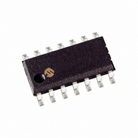
HCS515/SL Microchip Technology, HCS515/SL Datasheet - Page 11

HCS515/SL
Manufacturer Part Number
HCS515/SL
Description
IC CODE HOPPING DECODER 14-SOIC
Manufacturer
Microchip Technology
Type
Code Hopping Decoderr
Specifications of HCS515/SL
Applications
Remote Secure Access, Keyless Entry
Mounting Type
Surface Mount
Package / Case
14-SOIC (3.9mm Width), 14-SOL
Ic Function
Code Hopping Decoder IC
Supply Voltage Range
4.5V To 5.5V
Operating Temperature Range
0°C To +70°C
Digital Ic Case Style
SOIC
No. Of Pins
14
Termination Type
SMD
Filter Terminals
SMD
Rohs Compliant
Yes
Lead Free Status / RoHS Status
Lead free / RoHS Compliant
Other names
HCS515/SLR
HCS515/SLR
HCS515/SLR
Available stocks
Company
Part Number
Manufacturer
Quantity
Price
Company:
Part Number:
HCS515/SL
Manufacturer:
MICROCHIP
Quantity:
12 000
4.2.5
The read command (Figure 4-4) is used to read bytes
from the user EEPROM. The offset in the user
EEPROM is specified by the address byte, which is
truncated to 7 bits (C to D). After the address, a dummy
byte must be clocked in (D to E). The EEPROM data
byte is clocked out on the next rising edge of the clock
line with the Least Significant bit first (E to F). Sequen-
tial reads are possible by repeating sequence E to F
within 1 ms after the falling edge of the previous byte’s
Most Significant bit (MSb). During the sequential read,
the address value will wrap after 128 bytes. The
decoder will terminate the read command if no clock
pulses are received for a period longer than 1.2 ms.
FIGURE 4-4:
FIGURE 4-5:
Decoder DATA
2002 Microchip Technology Inc.
Decoder DATA
C DATA
C DATA
CLK
READ BYTE/S FROM USER
EEPROM
CLK
A
START Command
A
START Command
READ BYTES FROM USER EEPROM
WRITE BYTES TO USER EEPROM
B
B
LSB
LSB
Command Byte
Command Byte
MSB
MSB
C
C
LSB
LSB
Address Byte
Address Byte
MSB
4.2.6
The write command (Figure 4-5) is used to write a loca-
tion in the user EEPROM. The address byte is trun-
cated to seven bits (C to D). The data is clocked in
Least Significant bit (LSb) first. The clock line must be
asserted to initiate the write. Sequential writes of bytes
are possible by clocking in the byte and then asserting
the clock line (D – F). The decoder will terminate the
write command if no clock pulses are received for a
period longer than 1.2 ms After a successful write
sequence, the decoder will acknowledge by taking the
data line high and keeping it high until the clock line
goes low.
MSB
D
D
LSB
LSB
WRITE BYTE/S TO USER EEPROM
Data Byte
Dummy Byte
MSB
MSB
T
T
WR
RD
E
E
LSB
HCS515
Acknowledge
T
Data Byte
ACK
DS40183D-page 11
T
T
RESP
ACK
2
MSB
T
RD
F
F


