LX5261CDP Microsemi Analog Mixed Signal Group, LX5261CDP Datasheet - Page 2
LX5261CDP
Manufacturer Part Number
LX5261CDP
Description
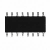
IC REG SCSI 27LINE LVD 16SOIC
Manufacturer
Microsemi Analog Mixed Signal Group
Datasheet
1.LX5261CDP.pdf
(6 pages)
Specifications of LX5261CDP
Applications
*
Mounting Type
Surface Mount
Package / Case
16-SOIC (3.9mm Width)
Lead Free Status / RoHS Status
Contains lead / RoHS non-compliant


Copyright © 2000
Rev. 1.0c, 2005-02-08
Term Power (VTERM) .........................................................................................................6V
Operating Junction Temperature..................................................................................... 150°C
Storage Temperature Range..............................................................................-65°C to 150°C
RoHS / Pb-freePeak Package Solder Reflow Temperature
(40 second maximum exposure) ........................................................................ 260°C (+0, -5)
Note:
Junction Temperature Calculation: T
The θ
system. All of the above assume no ambient airflow. θ
depending on mounting technique. (See Application Notes Section: Thermal
considerations)
T
HERMAL
DP
Exceeding these ratings could cause damage to the device. All voltages are with respect to Ground.
Currents are positive into, negative out of specified terminal.
JA
TM
numbers are guidelines for the thermal performance of the device/pc-board
P
DIFSENS
IN
VTERM
HSGND
VOUT1
VOUT2
16-Pin SOIC
R
GND
ESISTANCE
N
AME
A B S O L U T E M A X I M U M R A T I N G S
11861 Western Avenue, Garden Grove, CA. 92841, 714-898-8121, Fax: 714-893-2570
-J
UNCTION TO
T H E R M A L D A T A
J
= T
1.75V Regulated Output. Capable of sourcing/sinking 200mA.
0.75V Regulated Output. Capable of sourcing/sinking 200mA.
Power supply pin for terminator. Connect to SCSI bus VTERM. Usually decoupled
by one 4.7
decoupling capacitor through a very low impedance (big traces to PCB). Keeping distances
very short from the decoupling capacitors is somewhat layout dependent and some
applications may benefit from high frequency decoupling with 0.1
pin.
1.3V buffered output for DIFSENS signaling.
Regulator ground pin. Connect to ground.
Attached to die mounting pad, but not bonded to GND pin. Pins should be considered a
heat sink only, and not a true ground connection. It is recommended that these pins be
connected to ground, but can be left floating.
F U N C T I O N A L P I N D E S C R I P T I O N
A
+ (P
A
MBIENT
D
x θ
Integrated Products Division
µ
JA
F low-ESR capacitor. It is absolutely necessary to connect this pin to the
, θ
).
JA
®
JA
Microsemi
can vary significantly
27-Line LVD SCSI Source/Sink Regulator
111.8 °C/W
D
ESCRIPTION
P
RODUCTION
D
RoHS / Pb-free 100% Matte Tin Lead
ATA
DIFSENS
P A C K A G E P I N O U T
VTERM
HSGND
VOUT2
VOUT1
GND
S
N/C
N/C
NC – No Internal Connection
µ
HEET
F capacitors at VTERM
DP P
1
2
3
4
5
6
7
8
(Top View)
Finish
ACKAGE
16
15
14
13
12
11
10
LX5261
9
N/C
N/C
N/C
HSGND
HSGND
N/C
N/C
N/C
Page 2
Related parts for LX5261CDP
Image
Part Number
Description
Manufacturer
Datasheet
Request
R

Part Number:
Description:
IC USB LINE TERM EMI/ESD SC70-6
Manufacturer:
Microsemi Analog Mixed Signal Group
Datasheet:

Part Number:
Description:
IC USB LINE TERM EMI/ESD SC70-6
Manufacturer:
Microsemi Analog Mixed Signal Group
Datasheet:

Part Number:
Description:
IC TERM SCSI 9LINE MODE 24TSSOP
Manufacturer:
Microsemi Analog Mixed Signal Group
Datasheet:

Part Number:
Description:
IC TERM SCSI 9LINE MODE 28TSSOP
Manufacturer:
Microsemi Analog Mixed Signal Group
Datasheet:

Part Number:
Description:
IC TERM SCSI 9LINE LVD 24TSSOP
Manufacturer:
Microsemi Analog Mixed Signal Group
Datasheet:
Part Number:
Description:
IC TERM SCSI 9LINE MODE 36QSOP
Manufacturer:
Microsemi Analog Mixed Signal Group
Datasheet:

Part Number:
Description:
IC USB LINE TERM EMI/ESD SOT23-6
Manufacturer:
Microsemi Analog Mixed Signal Group
Datasheet:

Part Number:
Description:
IC USB LINE TERM EMI/ESD SOT23-6
Manufacturer:
Microsemi Analog Mixed Signal Group
Datasheet:

Part Number:
Description:
IC USB EMI FLTR ESD PROT SOT23-6
Manufacturer:
Microsemi Analog Mixed Signal Group
Part Number:
Description:
IC USB LINE TERM EMI/ESD SOT23-6
Manufacturer:
Microsemi Analog Mixed Signal Group
Datasheet:
Part Number:
Description:
IC AMP AUDIO PWR 10W STER 44SSOP
Manufacturer:
Microsemi Analog Mixed Signal Group
Datasheet:

Part Number:
Description:
IC CHARGER BATT USB LI-ION 20MLP
Manufacturer:
Microsemi Analog Mixed Signal Group
Datasheet:

Part Number:
Description:
IC LED DRIVER LINEAR 6-MLP
Manufacturer:
Microsemi Analog Mixed Signal Group
Datasheet:

Part Number:
Description:
IC LED DRIVR WT/CLR BCKLGT 8-MLP
Manufacturer:
Microsemi Analog Mixed Signal Group
Datasheet:

Part Number:
Description:
IC LED DRVR WT/CLR BCKLGT 8-MSOP
Manufacturer:
Microsemi Analog Mixed Signal Group
Datasheet: