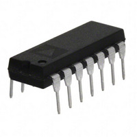
PKD01FP Analog Devices Inc, PKD01FP Datasheet - Page 12

PKD01FP
Manufacturer Part Number
PKD01FP
Description
IC MONO PEAK DETECTOR R&H 14-DIP
Manufacturer
Analog Devices Inc
Datasheet
1.PKD01FP.pdf
(18 pages)
Specifications of PKD01FP
Rohs Status
RoHS non-compliant
Applications
*
Mounting Type
Through Hole
Package / Case
14-DIP (0.300", 7.62mm)
Power Supply Requirement
Dual
Single Supply Voltage (typ)
Not RequiredV
Single Supply Voltage (min)
Not RequiredV
Single Supply Voltage (max)
Not RequiredV
Operating Temperature Classification
Commercial
Mounting
Through Hole
Pin Count
14
Package Type
PDIP
Lead Free Status / RoHS Status
Not Compliant
Available stocks
Company
Part Number
Manufacturer
Quantity
Price
Company:
Part Number:
PKD01FPZ
Manufacturer:
ENTROPIC
Quantity:
101
Part Number:
PKD01FPZ
Manufacturer:
ADI/亚德诺
Quantity:
20 000
PKD01
APPLICATIONS INFORMATION
Optional Offset Voltage Adjustment
Offset voltage is the primary zero scale error component since a
variable voltage clamp limits voltage excursions at D
and reduces charge injection. The PKD01 circuit gain and opera-
tional mode (positive or negative peak detection) determine the
applicable null circuit. Figures 5 through 8 are suggested circuits.
Each circuit also corrects amplifier C offset voltage error.
25k
V
V
NOTES:
1. NULL RANGE =
2. DISCONNECT R
3. REPEAT NULL CIRCUIT FOR RESET BUFFER AMPLIFIER B IF REQUIRED.
V
V
NOTES:
1. NULL RANGE =
2. DISCONNECT R
3. REPEAT NULL CIRCUIT FOR RESET BUFFER AMPLIFIER B IF REQUIRED.
IN
V
V
IN
S
IN
S
S
0.1 F
+
+
–
+
–
+
R
A
, R
100k
B
20k
R1
R1
0.1 F
AND R
R5
2M
1k
R1
R2
V
C
S
–
20
C
R3
R4
NOT NECESSARY FOR AMPLIFIER B ADJUSTMENT.
C
V
FROM C
V
FROM C
S
S
( )(
( )
R5
R4
R1
R2
DET
RST
H
A
B
H
R1 + R3
AFTER AMPLIFIER A ADJUSTMENT.
AFTER AMPLIFIER A ADJUSTMENT.
DET
RST
R1
A
B
D
)
1
D
1k
R2 = R3 + R4
R1
1
1000pF
C
H
1000pF
C
PKD01
H
C
PKD01
C
2M
R
C
1
2M
’s anode
–15V
R
C
200k
R
R
1k
V
–15V
A
B
OUT
200k
R
R
1k
V
A
B
OUT
A. Nulling Gated Output g
be conducting to close the feedback circuit during amplifier A
V
slightly. With DET = 0 and V
output. Adjust the null potentiometer until V
adjustment, disconnect R
B. Nulling Gated g
input to V
1, RST = 1 and adjust the null potentiometer for V
The circuit gain—inverting or noninverting—will determine which
null circuit illustrated in Figures 5 through 8 is applicable.
25k
25k
OS
V
V
IN
IN
V
V
V
V
NOTES:
1. NULL RANGE =
2. DISCONNECT R
3. REPEAT NULL CIRCUIT FOR RESET BUFFER AMPLIFIER B IF REQUIRED.
NOTES:
1. NULL RANGE =
2. DISCONNECT R
3. REPEAT NULL CIRCUIT FOR RESET BUFFER AMPLIFIER B IF REQUIRED.
adjustment. Resistor network R
S
S
S
S
+
–
–
+
R4 = R2 R1
IN
0.1 F
20k
R1
R5
= 0 V and monitor the PKD01 output. Set DET =
20k
0.1 F
R1 + R2
R3
R4
R3
20
C
C
R1
V
FROM C
V
FROM C
20
R4
S
S
m
( )
( )
R4
R3
R3
R5
Amplifier B. Set Amplifier B signal
H
H
C
AFTER AMPLIFIER A ADJUSTMENT.
AFTER AMPLIFIER A ADJUSTMENT.
from C
DET
RST
DET
RST
B
B
A
A
m
IN
Amplifier A. Diode D
= 0 V, monitor the PKD01
D
D
H
1
1
.
A
– R
R2
R2
C
1000pF
1000pF
C
H
H
C
cause D
PKD01
PKD01
C
C
OUT
= 0 V. After
GAIN = 1 +
1
OUT
to conduct
2M
2M
R
R
C
1
C
= 0 V.
must
–15V
–15V
R1 + R3
R
200k
1k
200k
R
R
R
1k
V
R2
V
A
B
A
B
OUT
OUT


