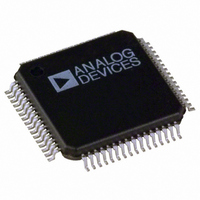
AD5520JST Analog Devices Inc, AD5520JST Datasheet - Page 19

AD5520JST
Manufacturer Part Number
AD5520JST
Description
IC SNGL PARAMETRIC MEASURE64LQFP
Manufacturer
Analog Devices Inc
Type
Per-pin Parametric Measurement Unit (PPMU)r
Datasheet
1.AD5520JSTZ.pdf
(24 pages)
Specifications of AD5520JST
Rohs Status
RoHS non-compliant
Applications
Automatic Test Equipment
Mounting Type
Surface Mount
Package / Case
64-LQFP
Operating Temperature (min)
0C
Operating Temperature (max)
70C
Operating Temperature Classification
Commercial
Mounting
Surface Mount
For Use With
EVAL-AD5520EBZ - BOARD EVAL FOR AD5520
Lead Free Status / RoHS Status
Not Compliant
Available stocks
Company
Part Number
Manufacturer
Quantity
Price
Company:
Part Number:
AD5520JST
Manufacturer:
ADI
Quantity:
150
Part Number:
AD5520JST
Manufacturer:
ADI/亚德诺
Quantity:
20 000
Company:
Part Number:
AD5520JSTZ
Manufacturer:
Analog Devices Inc
Quantity:
10 000
Part Number:
AD5520JSTZ
Manufacturer:
ADI/亚德诺
Quantity:
20 000
PCB LAYOUT AND POWER SUPPLY DECOUPLING
In any circuit where accuracy is important, careful considera-
tion to the power supply and the ground return layout helps to
ensure the rated performance. The printed circuit board on
which the AD5520 is mounted should be designed so that the
analog and digital sections are separated and confined to
certain areas of the board. If the PMU is in a system where
multiple devices require an AGND-to-DGND connection, the
connection should be made at one point only. The star ground
point should be established as close as possible to the device.
This PMU should have ample supply bypassing of 10 μF in
parallel with 0.1 μF on the supply and should be located as close
as possible to the package, ideally right up against the device. The
0.1 μF capacitor should have low effective series resistance (ESR)
and effective series inductance (ESI), such as the common
ceramic types that provide a low impedance path to ground at
high frequencies, to handle transient currents due to internal
logic switching. Low ESR (1 μF to 10 μF) tantalum or electrolytic
capacitors should also be applied at the supplies to minimize
transient disturbance and filter out low frequency ripple.
Rev. B | Page 19 of 24
Fast switching signals, such as clocks, should be shielded with
digital ground to avoid radiating noise to other parts of the
board and should never be run near the reference inputs.
Avoid crossover of digital and analog signals. Traces on
opposite sides of the board should run at right angles to each
other. This reduces the effects of feedthrough through the
board. A microstrip technique is by far the best but not always
possible with a double-sided board. In this technique, the
component side of the board is dedicated to the ground plane
while signal traces are placed on the solder side.
It is good practice to use compact, minimum lead length PCB
layout design. Leads to the input should be as short as possible
to minimize IR drops and stray inductance.
AD5520


