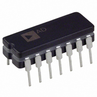
PKD01FY Analog Devices Inc, PKD01FY Datasheet - Page 11

PKD01FY
Manufacturer Part Number
PKD01FY
Description
IC MONO PEAK DETECTOR R&H 14CDIP
Manufacturer
Analog Devices Inc
Datasheet
1.PKD01FP.pdf
(18 pages)
Specifications of PKD01FY
Rohs Status
RoHS non-compliant
Applications
*
Mounting Type
Through Hole
Package / Case
14-CDIP (0.300", 7.62mm)
Power Supply Requirement
Dual
Single Supply Voltage (typ)
Not RequiredV
Single Supply Voltage (min)
Not RequiredV
Single Supply Voltage (max)
Not RequiredV
Operating Temperature Classification
Commercial
Mounting
Through Hole
Pin Count
14
Lead Free Status / RoHS Status
Not Compliant
Available stocks
Company
Part Number
Manufacturer
Quantity
Price
THEORY OF OPERATION
The typical peak detector uses voltage amplifiers and a diode or
an emitter follower to charge the hold capacitor, C
ionally (see Figure 1). The output impedance of A plus D
dynamic impedance, r
mines the feedback loop pole. The dynamic impedance is
The pole moves toward the origin of the S plane as I
zero. The pole movement in itself will not significantly lengthen
the acquisition time since the pole is enclosed in the system
feedback loop.
When the moving pole is considered with the typical frequency
compensation of voltage amplifiers however, there is a loop stability
problem. The necessary compensation can increase the required
acquisition time. ADI’s approach replaces the input voltage ampli-
fier with a transconductance amplifier (see Figure 2).
The PKD01 transfer function can be reduced to:
where: g
The diode in series with A’s output (see Figure 2) has no effect
because it is a resistance in series with a current source. In
addition to simplifying the system compensation, the input
transconductance amplifier output current is switched by cur-
rent steering. The steered output is clamped to reduce and match
any charge injection.
Figure 3 shows a simplified schematic of the reset g
B. In the track mode, Q
OFF. A current of 2I passes through D
passes through Q
can absorb only 3I, thus the current passing through D
r
d
=
INPUT
kT
qI
INPUT
V
V
IN
IN
d
m
, where I
V
1 µA/mV, R
V
I
OUT
V
OUT
R
V
I
IN
OUT
OUT
OUT
OUT
1
+
d
, and is summed with g
(A) = V
(A) = V
=
is the capacitor charging current.
R
A
OUT
A
1
+
d
IN
, make up the resistance which deter-
IN
OUT
sC
1
(A)
(A)
g
and Q
m
H
g
D
D
A
+
m
1
1
1
V
20 MΩ.
(A)
r
g R
(A)
d
4
m
V
are ON and Q
V
H
1
H
C
OUT
C
H
H
1
, I is summed at B and
m
≈
C
V
C
1
IN
+
. The current sink
V
1
sC
OUT
g
m
2
H
and Q
m
OUTPUT
H
OUTPUT
amplifier,
, indirect-
d
goes to
2
3
are
can
1
’s
only be: 2K – g
node then, is g
Q
into the top of D
bottom of D
thus, D
tion is independent of input level.
The monolithic layout results in points A and B having equal
nodal capacitance. In addition, matched diodes D
equal diffusion capacitance. When the transconductance ampli-
fier outputs are switched open, points A and B are ramped
equally, but in opposite phase. Diode clamps D
the swings to have equal amplitudes. The net charge injection
(voltage change) at node C is therefore zero.
The peak transconductance amplifier, A is shown in Figure 4.
Unidirectional hold capacitor charging requires diode D
connected in series with the output. Upon entering the peak
hold mode D
injection to approximately 1 pC and the hold step to 0.6 mV.
Minimizing acquisition time dictates a small C
1000 pF value was selected. Droop rate was also minimized by
providing the output buffer with an FET input stage. A cur-
rent cancellation circuit further reduces droop current and
minimizes the gate current’s tendency to double for every 10°
temperature change.
2
and Q
V
V
IN
IN
1
and D
3
are ON while Q
2
1
is pulled up with a current I until D
m
is reverse-biased. The voltage clamp limits charge
2
m
V
g
g
1
are reverse biased by <0.6 V, and charge injec-
m
m
I
I
IN
V
is –I until D
A
C
B
V
V
IN
Q
Q
[I
IN
IN
1
1
. The net current into the hold capacitor
D
D
D
H
2I
2I
2
1
2
Q
Q
V+
V+
= 2I – (2I – g
3I
3I
2
2
D
1
1
r
6
6
d
and Q
3
Q
Q
3
3
turns ON. With Q
D
D
D
D
3
3
4
4
Q
Q
4
3I
3I
4
4
are OFF. The net current
m
V–
V–
V
C
C
IN
H
H
)]. In the hold mode,
A > B = PEAK DETECT
A < B = PEAK HOLD
A > B = PEAK DETECT
A < B = PEAK HOLD
C
C
A
B
A
B
H
3
LOGIC
CONTROL
LOGIC
CONTROL
capacitance. A
PKD01
and D
4
1
1
turns ON,
and D
OFF, the
4
1
cause
to be
2
have


