IL611-2E NVE, IL611-2E Datasheet - Page 6
IL611-2E
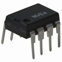
Manufacturer Part Number
IL611-2E
Description
ISOLATOR PASSIVE INPUT HS 8DIP
Manufacturer
NVE
Series
IsoLoop®r
Datasheet
1.IL610-1E.pdf
(21 pages)
Specifications of IL611-2E
Inputs - Side 1/side 2
2/0
Number Of Channels
2
Isolation Rating
2500Vrms
Voltage - Supply
3 V ~ 5.5 V
Data Rate
100Mbps
Propagation Delay
12ns
Output Type
CMOS
Package / Case
8-DIP
Operating Temperature
-40°C ~ 85°C
No. Of Channels
2
Supply Current
4mA
Supply Voltage Range
3V To 5.5V
Digital Ic Case Style
DIP
No. Of Pins
8
Operating Temperature Range
-40°C To +85°C
Lead Free Status / RoHS Status
Lead free / RoHS Compliant
Other names
390-1082-5


Electrical specifications are T
Notes:
Parameters
Quiescent Current
Logic High Output Voltage
Logic Low Output Voltage
Logic Output Drive Current
Failsafe Operation Input Current
Input Signal Rise and Fall Times
Data Rate
Minimum Pulse Width
Propagation Delay Input to Output
(High to Low)
Propagation Delay Input to Output
(Low to High)
Average Propagation Delay Drift
Pulse Width Distortion |t
Propagation Delay Skew
Output Rise Time (10–90%)
Output Fall Time (10–90%)
Common Mode Transient Immunity
1.
2.
3.
4.
The Minimum Pulse Width is the shortest pulse width at which the specified PWD is guaranteed.
PWD is defined as | t
t
Failsafe Operation is defined as the guaranteed output state which will be achieved if the DC input current falls between the input levels specified
(see Test Circuit 1 for details). Note if Failsafe to Logic Low is required, the DC current supplied to the coil must be at least 8 mA using 3.3 V supplies
versus 5 mA for 5 V supplies. Select the value of limit resistor appropriately.
PSK
is equal to the magnitude of the worst case difference in t
(1)
PHL
(3)
−t
PHL −
min
PLH
to T
|
t
(4)
PLH
(2)
max
|.
and 3.0V to 3.6V unless otherwise stated.
|CM
IL612, I
IL612, I
IL614, I
IL614, I
IL610, I
IL611, I
IL613, I
Symbol
I
I
FS-HIGH
FS-LOW
PWD
t
V
V
IR
PW
t
t
t
t
H
|I
PHL
PLH
PLH
PSK
t
t
|,|CM
, t
OH
OL
O
R
F
|
IF
DD1
DD2
DD1
DD2
Switching Specifications at 3.3V
DD
DD
DD
L
|
PHL
Min.
−25
100
3.2
3.0
and/or t
10
−2
15
7
8
6
PLH
that will be seen between units at 25°C.
Typ.
1.3
2.6
1.3
1.3
1.3
2.6
3.3
3.1
0.2
10
12
12
10
20
4
0
3
3
3
Max.
0.1
0.8
0.3
25
18
18
2
4
2
2
6
2
4
1
5
2
5
5
kV/µs
Units
Mbps
ps/°C
mA
mA
mA
mA
mA
mA
mA
mA
mA
mA
IL600 Series
µs
ns
ns
ns
ns
ns
ns
ns
V
V
Test Conditions
V
V
V
V
V
See Test Circuit 1
See Test Circuit 1
See Test Circuit 1
See Test Circuit 1
See Test Circuit 1
See Test Circuit 1
See Test Circuit 1
See Test Circuit 1
See Test Circuit 1
See Test Circuit 1
V
DD
DD
DD
DD
DD
T
= 300 V
= 3.3 V, I
= 3.3 V, I
= 3.3 V, I
= 3.3 V, I
= 3.3 V, I
peak
IN
O
O
O
O
= 20 µA
= 4 mA
= −20 µA
= −4 mA
= 0
Related parts for IL611-2E
Image
Part Number
Description
Manufacturer
Datasheet
Request
R

Part Number:
Description:
ISOLATOR PASSIVE INPUT HS 8SOIC
Manufacturer:
NVE
Datasheet:

Part Number:
Description:
ISOLATOR PASSIVE INPUT HS 8MSOP
Manufacturer:
NVE
Datasheet:


Part Number:
Description:
ISOLATOR HS MAG DIGITAL 8SOIC
Manufacturer:
NVE
Datasheet:
Part Number:
Description:
ISOLATOR HS DIGITAL 125C 8SOIC
Manufacturer:
NVE
Datasheet:

Part Number:
Description:
HI-SPD 4CHANN COUPLER 16-SOIC LF
Manufacturer:
NVE
Datasheet:
Part Number:
Description:
ISOLATOR HS MAG DIGITAL 16SOIC
Manufacturer:
NVE
Datasheet:
Part Number:
Description:
ISOLATOR HS MAG DIGITAL 8SOIC
Manufacturer:
NVE
Datasheet:

Part Number:
Description:
IC DIFFER BUS TRANSC 16 SOIC
Manufacturer:
NVE
Datasheet:
Part Number:
Description:
ISOLATOR HS MAG DIGITAL 16SOICW
Manufacturer:
NVE
Datasheet:

Part Number:
Description:
ISOLATOR RS422/485 INTFC 16SOICW
Manufacturer:
NVE
Datasheet: