ILQ620GB Vishay, ILQ620GB Datasheet
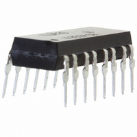
OPTOCPLR PHOTOTRA 4CH 100% 16DIP

ILQ620GB

Manufacturer Part Number
ILQ620GB
Description
OPTOCPLR PHOTOTRA 4CH 100% 16DIP
Manufacturer
Vishay
Datasheets

Specifications of ILQ620GB

Mounting Type
Through Hole
Isolation Voltage
5300 Vrms
Number Of Channels
4
Input Type
AC, DC
Voltage - Isolation
5300Vrms
Current Transfer Ratio (min)
100% @ 5mA
Current Transfer Ratio (max)
600% @ 5mA
Voltage - Output
70V
Current - Output / Channel
50mA
Current - Dc Forward (if)
±60mA
Vce Saturation (max)
400mV
Output Type
Transistor
Package / Case
16-DIP (0.300", 7.62mm)
Forward Current
60 mA
Maximum Input Diode Current
60 mA
Output Device
Transistor
Configuration
4
Maximum Collector Emitter Voltage
70 V
Maximum Collector Emitter Saturation Voltage
400 mV
Current Transfer Ratio
600 %
Maximum Forward Diode Voltage
1.3 V
Minimum Forward Diode Voltage
1 V
Maximum Collector Current
100 mA
Maximum Power Dissipation
500 mW
Maximum Operating Temperature
+ 100 C
Minimum Operating Temperature
- 55 C
No. Of Channels
4
Optocoupler Output Type
Phototransistor
Input Current
10mA
Output Voltage
70V
Opto Case Style
DIP
No. Of Pins
16
Lead Free Status / RoHS Status
Lead free / RoHS Compliant
Lead Free Status / RoHS Status
Lead free / RoHS Compliant, Lead free / RoHS Compliant
Other names
751-1332-5
ILQ620GBGI
ILQ620GBGI

Available stocks

Company
Part Number
Manufacturer
Quantity
Price
Part Number:
ILQ620GB
Manufacturer:
NS
Quantity:
99
Optocoupler, Phototransistor Output, AC Input (Dual, Quad
Channel)
Features
Agency Approvals
Description
The ILD620/ ILQ620 and ILD620GB/ ILQ620GB are
multi-channel input phototransistor optocouplers that
use inverse parallel GaAs IRLED emitter and high
gain NPN silicon phototransistors per channel. These
devices are constructed using over/under leadframe
optical coupling and double molded insulation result-
ing in a withstand test voltage of 5300 V
The LED parameters and the linear CTR characteris-
tics make these devices well suited for AC voltage
detection. the ILD/Q620GB with its low I
CTR
age detection network that is placed in series with the
LEDs. Eliminating the phototransistor base connec-
tion provides added electrical noise immunity from the
transients found in many industrial control environ-
ments.
Document Number 83653
Rev. 1.4, 26-Oct-04
• Identical Channel to Channel Footprint
• ILD620 Crosses to TLP620-2
• ILQ620 Crosses to TLP620-4
• High Collector-Emitter Voltage, BV
• Dual and Quad Packages Feature:
• Isolation Test Voltage 5300 V
• Lead-free component
• Component in accordance to RoHS 2002/95/EC
• UL1577, File No. E52744 System Code H or J,
• CSA 93751
• DIN EN 60747-5-2 (VDE0884)
• BSI IEC60950 IEC60065
and WEEE 2002/96/EC
Double Protection
DIN EN 60747-5-5 pending
Available with Option 1
- Reduced Board Space
- Lower Pin and Parts Count
- Better Channel to Channel CTR Match
- Improved Common Mode Rejection
CEsat
minimizes power dissipation of the AC volt-
RMS
CEO
F
RMS
quaranteed
ILD620/ 620GB / ILQ620/ 620GB
= 70 V
.
Order Information
For additional information on the available options refer to
Option Information.
ILD620
ILD620GB
ILQ620
ILQ620GB
ILD620-X007
ILD620-X009
ILD620GB-X009
ILQ620-X009
ILQ620GB-X009
i179053
Dual Channel
Quad Channel
Part
CTR > 50 %, DIP-8
CTR > 100 %, DIP-8
CTR > 50 %, DIP-16
CTR > 100 %, DIP-16
CTR > 50 %, SMD-8 (option 7)
CTR > 50 %, SMD-8 (option 9)
CTR > 100 %, SMD-8 (option 9)
CTR > 50 %, SMD-16 (option 9)
CTR > 100 %, SMD-16 (option 9)
Vishay Semiconductors
A/C
A/C
A/C
A/C
A/C
A/C
A/C
A/C
A/C
A/C
A/C
A/C
1
2
3
4
5
6
7
8
4
1
2
3
Remarks
16
15
14
13
12
11
10
8
6
5
7
9
e3
www.vishay.com
C
E
C
E
C
E
C
E
C
E
C
E
Pb
Pb-free
1

Related parts for ILQ620GB

ILQ620GB Summary of contents

Page 1

... DIN EN 60747-5-5 pending Available with Option 1 • BSI IEC60950 IEC60065 Description The ILD620/ ILQ620 and ILD620GB/ ILQ620GB are multi-channel input phototransistor optocouplers that use inverse parallel GaAs IRLED emitter and high gain NPN silicon phototransistors per channel. These devices are constructed using over/under leadframe ...

Page 2

... Test condition Symbol FSM P diss Test condition Symbol BV CEO diss Test condition Part ILD620 ILD620GB ILQ620 ILQ620GB = 25 °C amb = 100 °C amb Value Unit ± ± 1.5 A 100 mW 1.3 mW/°C Value Unit 100 mA 150 mW 2.0 mW/°C ...

Page 3

... ILQ620 = 0.2 mA ILD620GB CE ILQ620GB Test condition Part = 5 5.0 mA 5.0 mA) = 0.4 V ILD620 CE ILQ620 = 5.0 V ILD620 CE ILQ620 = 0.4 V ILD620GB CE ILQ620GB = 5.0 V ILD620GB CE ILQ620GB Vishay Semiconductors Min Typ. Max 1.0 1.15 1.3 2 750 Min Typ. Max 6.8 10 100 2.0 50 500 Symbol Min Typ. Max I 1 ...

Page 4

... ILD620/ 620GB / ILQ620/ 620GB Vishay Semiconductors Switching Characteristics Non-saturated Parameter On time I = ± Ω Rise time I = ± Ω Off time I = ± Ω Fall time I = ± Ω Propagation H ± Ω Propagation L ± Ω Saturated Parameter On time I = ± 10 mA, V ...

Page 5

... -60 -40 -20 iild620_07 Figure 7. Maximum LED Current vs. Ambient Temperature 200 150 100 –55 °C 50 1.0 1.5 0 -60 -40 -20 iild620_08 Figure 8. Maximum LED Power Dissipation Vishay Semiconductors Vce = 10 V Typical 100 Ambient Temperature - °C TJ (MAX) = 100 ° 100 Ta - Ambient Temperature - ° 100 Ta - Ambient Temperature - ° ...

Page 6

... ILD620/ 620GB / ILQ620/ 620GB Vishay Semiconductors 100 50 Normalized ILD/Q620GB 5.0 2.5 ILD/Q620 1.0 0.5 0 Forward Current - iild620_09 Figure 9. Collector Current vs. Diode Forward Current 2.0 Normalized to mA 1.5 CTRce(sat 0 NCTRce 1.0 NCTRce(sat) 0.5 0 LED Current - mA iild620_10 Figure 10. Normalization Factor for Non-saturated and Saturated CTR vs ...

Page 7

... Figure 15. Maximum Collector Current vs. Collector Voltage Rth = 500 °C/W 25 °C 50 °C 75 °C 90 °C 100 pin one ISO Method A .300 (7.62) .031 (0.79) typ. .130 (3.30) .150 (3.81) 10° .020 (.51 ) 3°–9° .035 (.89 ) .008 (.20) .012 (.30) Vishay Semiconductors .230(5.84) .110 (2.79) .250(6.35) .130 (3.30) www.vishay.com 7 ...

Page 8

... ILD620/ 620GB / ILQ620/ 620GB Vishay Semiconductors Package Dimensions in Inches (mm .779 (19.77 ) .790 (20.07) .030 (.76) .045 (1.14) 4° .018 (.46) .022 (.56) .100 (2.54)typ. i178007 Option 7 .300 (7.62) TYP . .028 (0.7) MIN. .315 (8.0) MIN. .331 (8.4) MIN. .406 (10.3) MAX. www.vishay.com 8 pin one ID ...

Page 9

... Various national and international initiatives are pressing for an earlier ban on these substances. Vishay Semiconductor GmbH has been able to use its policy of continuous improvements to eliminate the use of ODSs listed in the following documents. 1. Annex A, B and list of transitional substances of the Montreal Protocol and the London Amendments respectively 2 ...

Page 10

... Vishay disclaims any and all liability arising out of the use or application of any product described herein or of any information provided herein to the maximum extent permitted by law. The product specifications do not expand or otherwise modify Vishay’ ...

Related keywords