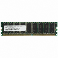
MT9VDDT6472AY-335F1 Micron Technology Inc, MT9VDDT6472AY-335F1 Datasheet - Page 22

MT9VDDT6472AY-335F1
Manufacturer Part Number
MT9VDDT6472AY-335F1
Description
MODULE DDR SDRAM 512MB 184-DIMM
Manufacturer
Micron Technology Inc
Datasheet
1.MT9VDDT6472AG-335D1.pdf
(27 pages)
Specifications of MT9VDDT6472AY-335F1
Memory Type
DDR SDRAM
Memory Size
512MB
Speed
333MT/s
Package / Case
184-DIMM
Lead Free Status / RoHS Status
Lead free / RoHS Compliant
Other names
557-1177
MT9VDDT6472AY-335F1
MT9VDDT6472AY-335F1
Available stocks
Company
Part Number
Manufacturer
Quantity
Price
Company:
Part Number:
MT9VDDT6472AY-335F1
Manufacturer:
MICRON
Quantity:
3 422
SPD Clock and Data Conventions
SCL LOW. SDA state changes during SCL HIGH are
reserved for indicating start and stop conditions (as
shown in Figure 10, Data Validity, and Figure 11, Defi-
nition of Start and Stop).
SPD Start Condition
which is a HIGH-to-LOW transition of SDA when SCL
is HIGH. The SPD device continuously monitors the
SDA and SCL lines for the start condition and will not
respond to any command until this condition has been
met.
SPD Stop Condition
tion, which is a LOW-to-HIGH transition of SDA when
SCL is HIGH. The stop condition is also used to place
the SPD device into standby power mode.
pdf: 09005aef80a43e7d, source: 09005aef80a43d77
DDA9C16_32_64x72AG.fm - Rev. B 9/04 EN
SCL from Master
Data Output
from Transmitter
Data Output
from Receiver
SDA
SCL
Data states on the SDA line can change only during
All commands are preceded by the start condition,
All communications are terminated by a stop condi-
Figure 10: Data Validity
DATA STABLE
Figure 12: Acknowledge Response from Receiver
DATA
CHANGE
DATA STABLE
128MB, 256MB, 512MB (x72, ECC, SR), PC3200
22
SPD Acknowledge
cate successful data transfers. The transmitting device,
either master or slave, will release the bus after trans-
mitting eight bits. During the ninth clock cycle, the
receiver will pull the SDA line LOW to acknowledge
that it received the eight bits of data (as shown in Fig-
ure 11, Definition of Start and Stop).
acknowledge after recognition of a start condition and
its slave address. If both the device and a WRITE oper-
ation have been selected, the SPD device will respond
with an acknowledge after the receipt of each subse-
quent eight-bit word. In the read mode the SPD device
will transmit eight bits of data, release the SDA line and
monitor the line for an acknowledge. If an acknowl-
edge is detected and no stop condition is generated by
the master, the slave will continue to transmit data. If
an acknowledge is not detected, the slave will termi-
nate further data transmissions and await the stop
condition to return to standby power mode.
Figure 11: Definition of Start and Stop
SDA
SCL
Acknowledge is a software convention used to indi-
The SPD device will always respond with an
Micron Technology, Inc., reserves the right to change products or specifications without notice.
184-Pin DDR SDRAM UDIMM
START
BIT
8
Acknowledge
©2004 Micron Technology, Inc.
9
STOP
BIT


