DLG2416 OSRAM Opto Semiconductors Inc, DLG2416 Datasheet - Page 8
DLG2416
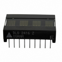
Manufacturer Part Number
DLG2416
Description
INTELLIGENT DISP 4CHAR 5X7 GRN
Manufacturer
OSRAM Opto Semiconductors Inc
Datasheet
1.DLG2416.pdf
(11 pages)
Specifications of DLG2416
Size / Dimension
1.00" L x 0.80" W x 0.26" H (25.40mm x 20.32mm x 6.60mm)
Color
Green
Number Of Digits
4
Character Size
0.2 in
Illumination Color
Green
Wavelength
565 nm
Maximum Operating Temperature
+ 85 C
Minimum Operating Temperature
- 40 C
Luminous Intensity
120 ucd
Viewing Area (w X H)
3.45 mm x 5.03 mm
Display Type
5 x 7 Dot Matrix
Lead Free Status / RoHS Status
Lead free / RoHS Compliant
Configuration
-
Voltage - Forward (vf) Typ
-
Millicandela Rating
-
Internal Connection
-
Lead Free Status / Rohs Status
Details
Other names
475-1352
DLG2416
Q68000A8096
DLG2416
Q68000A8096


Loading Data
Setting the chip enable (CE1, CE2) to their true state will
enable data loading. The desired data code (D0-D6) and
digit address (A0, A1) must be held stable during the
write cycle for storing new data.
Data entry may be asynchronous and random. Digit 0 is
defined as right hand digit with A1=A2=0.
To clear the entire internal four-digit memory hold the
clear (CLR) low for 1.0 µs. All illuminated dots will be
turned off within one complete display multiplex cycle,
1.0 ms minimum. The clear function will clear both the
ASCII RAM and the cursor RAM.
Loading Cursor
Setting the chip enables (CE1, CE2) and cursor select
(CU) to their true state will enable cursor loading. A write
(WR) pulse will now store or remove a cursor into the
digit location addressed by A0, A1, as defined in data
entry. A cursor will be stored if D0=1 and will removed if
D0=0. The cursor (CU) pulse width should not be less
than the write (WR) pulse or erroneous data may appear
in the display.
If the cursor is not required, the cursor enable signal
(CUE) may be tied low to disable the cursor function. For
a flashing cursor, simply pulse CUE. If the cursor has
been loaded to any or all positions in the display, then
CUE will control whether the cursor(s) or the characters
will appear. CUE does not affect the contents of cursor
memory.
Display Blanking
Blanking the display may be accomplished by loading a
blank or space into each digit of the display or by using
the (BL) display blank input.
Setting the (BL) input low does not affect the contents of
either data or cursor memory.
A flashing circuit can easily be constructed using a 555
as table multivibrator. Figure 4 illustrates a circuit in
which varying R2 (100K~10K) will have a flash rate of
1.0 Hz~10 Hz.
The display can be dimmed by pulse width modulating
the (BL) at a frequency sufficiently fast to not interfere
with the internal clock. The dimming signal frequency
should be 2.5 kHz or higher. Dimming the display also
reduces power consumption.
An example of a simple dimming circuit using a 556 is
illustrated in Figure 5. Adjusting potentiometer R3 will
dim the display by changing the blanking pulse duty
cycle.
Design Considerations
For details on design and applications of the DLX2416
using standard bus configurations in multiple display sys-
tems, or parallel I/O devices, such as the 8255 with an
8080 or memory mapped addressing on processors such
as the 8080, Z80, 6502, or 6800, refer to Appnote 14 at
www.osram-os.com.
2006-01-23
8
DLX2416—Flashing Circuit Using a 555 and
Flashing (Blanking) Timing
DLX2416—Dimming Circuit Using a 556 and
Dimming (Blanking) Timing
1
0
To BL
Pin on
Display
1
0
~ ~
~ ~
2 Hz Blanking Frequency
R
47 k
R
200
C
4700 pF
5 kHz Blanking Frequency
2
1
1
Ω
Ω
C
0.01 µF
2
DLR2416, DLO2416, DLG2416
~ ~
~ ~
500 ms
200 µs
Dimming (Blanking)
1
2
3
4
5
6
7
1
2
3
4
Dual Timer
Control
556
Timer
555
14
13
12
11
10
9
8
Blanking Pulse Width
~ ~
8
7
6
5
50% Duty Factor
Blanking Pulse Width
4 µs min., 196 µs max.
C
0.01 µF
4
V
C
1000 pF
C
0.01 µF
CC
500 k
IDCD5034
R
3
4
3
= 5 V
Ω
IDCD5035
To BL Pin
on Display
IDCD5036
V
4.7 k
R
C
10 µF
CC
IDCD5033
1
100 k
R
3
2
= 5 V
Ω
Ω
Related parts for DLG2416
Image
Part Number
Description
Manufacturer
Datasheet
Request
R

Part Number:
Description:
INTELLIGENT DISP 4CHAR 5X7 HERED
Manufacturer:
OSRAM Opto Semiconductors Inc
Datasheet:

Part Number:
Description:
DISPLAY 8DIGIT CERAMIC GREEN
Manufacturer:
OSRAM Opto Semiconductors Inc
Datasheet:

Part Number:
Description:
EMITTER IR 950NM 5MM SMD RADIAL
Manufacturer:
OSRAM Opto Semiconductors Inc
Datasheet:

Part Number:
Description:
LED TOPLED GREEN 570NM 2-PLCC
Manufacturer:
OSRAM Opto Semiconductors Inc
Datasheet:

Part Number:
Description:
INTERRUPTER RELFECT W/FILTR SMD
Manufacturer:
OSRAM Opto Semiconductors Inc
Datasheet:

Part Number:
Description:
LED Displays 5x7 Green 0.145 , 4-CHARACTER
Manufacturer:
OSRAM Opto Semiconductors Inc
Datasheet:

Part Number:
Description:
Q65110A4321_SIDELED PURE GREEN EOL150407
Manufacturer:
OSRAM Opto Semiconductors Inc
Datasheet:
Part Number:
Description:
Q65110A1202_RO DETECTOR 3/5MM_TR_RO
Manufacturer:
OSRAM Opto Semiconductors Inc
Datasheet:

Part Number:
Description:
PHOTODIODE 900NM 3MM W/FILTER
Manufacturer:
OSRAM Opto Semiconductors Inc
Datasheet:
Part Number:
Description:
INTELLIGENT DISP 4CHAR 5X7 HERED
Manufacturer:
OSRAM Opto Semiconductors Inc
Datasheet:
Part Number:
Description:
LED TOPLED GREEN 570NM 2-PLCC
Manufacturer:
OSRAM Opto Semiconductors Inc
Datasheet:
Part Number:
Description:
PHOTODIODE 900NM 3MM W/FILTER
Manufacturer:
OSRAM Opto Semiconductors Inc
Datasheet:

Part Number:
Description:
PHOTODIODE 850NM THRU-HOLE
Manufacturer:
OSRAM Opto Semiconductors Inc
Datasheet:

Part Number:
Description:
PHOTODIODE 880NM W/FILTER SMD
Manufacturer:
OSRAM Opto Semiconductors Inc
Datasheet: