591-2404-013F Dialight, 591-2404-013F Datasheet - Page 8
591-2404-013F
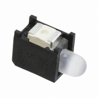
Manufacturer Part Number
591-2404-013F
Description
LED YELLOW PRISM/CBI 587NM SMD
Manufacturer
Dialight
Series
Prism®, CBI®r
Specifications of 591-2404-013F
Color
Yellow
Voltage Rating
1.8V
Current
20mA
Lens Style/size
Round, 2.84mm
Configuration
Single
Mounting Type
Surface Mount
Lead Free Status / RoHS Status
Lead free / RoHS Compliant
Lens Type
-
Other names
350-2315-2


Valid Data Indicator (QVLD)
QVLD is provided on the DDR II+ to simplify data capture on high
speed systems. The QVLD is generated by the DDR II+ device
along with data output. This signal is also edge aligned with the
echo clock and follows the timing of any data pin. This signal is
asserted half a cycle before valid data arrives.
On-Die Termination (ODT)
These devices have an On-Die Termination feature for Data
inputs (D
and K). The termination resistors are integrated within the chip.
The ODT range selection is enabled through ball R6 (ODT pin).
The ODT termination tracks value of RQ where RQ is the resistor
tied to the ZQ pin. ODT range selection is made during power up
initialization. A LOW on this pin selects a low range that follows
RQ/3.33 for 175Ω < RQ < 350Ω (where RQ is the resistor tied to
ZQ pin). A HIGH on this pin selects a high range that follows
RQ/1.66 for 175Ω < RQ < 250Ω (where RQ is the resistor tied to
ZQ pin). When left floating, a high range termination value is
Application Example
Figure 1
Document Number: 001-57344 Rev. *A
(CPU or ASIC)
Echo Clock1/Echo Clock1
Echo Clock2/Echo Clock2
MASTER
[x:0]
shows two DDR II+ used in an application.
BUS
), Byte Write Selects (BWS
Source CLK
Source CLK
Addresses
BWS
ODT
R/W
DQ
LD
DQ
[x:0]
A
), and Input Clocks (K
LD
SRAM#1
R/W BWS
Figure 1. Application Example
CQ/CQ
K
ODT
ZQ
K
R = 250ohms
selected by default. For a detailed description on the ODT imple-
mentation, refer to the application note, On-Die Termination for
QDRII+/DDRII+ SRAMs.
PLL
These chips use a PLL that is designed to function between 120
MHz and the specified maximum clock frequency. During power
up, when the DOFF is tied HIGH, the PLL is locked after 20 μs
of stable clock. The PLL can also be reset by slowing or stopping
the input clock K and K for a minimum of 30 ns. However, it is not
necessary to reset the PLL to lock to the desired frequency. The
PLL automatically locks 20 μs after a stable clock is presented.
The PLL may be disabled by applying ground to the DOFF pin.
When the PLL is turned off, the device behaves in DDR I mode
(with one cycle latency and a longer access time). For infor-
mation, refer to the application note, PLL Considerations in
QDRII/DDRII/QDRII+/DDRII+.
DQ
A
LD
SRAM#2
R/W BWS
CY7C21701KV18
CQ/CQ
K
ODT
ZQ
K
R = 250ohms
Page 8 of 24
[+] Feedback
Related parts for 591-2404-013F
Image
Part Number
Description
Manufacturer
Datasheet
Request
R

Part Number:
Description:
LED PRISM 3MM RND LC SQ YLW SMD
Manufacturer:
Dialight
Datasheet:
Part Number:
Description:
LED PRISM 3MM RND LC YLW SMD
Manufacturer:
Dialight
Datasheet:
Part Number:
Description:
LED PRISM 3MM RND LC SQ YLW SMD
Manufacturer:
Dialight
Datasheet:
Part Number:
Description:
LED PRISM 3MM RND LC YLW SMD
Manufacturer:
Dialight
Datasheet:
Part Number:
Description:
LED PRISM 3MM RND LC SQ YLW SMD
Manufacturer:
Dialight
Datasheet:

Part Number:
Description:
LED PRISM 3MM GREEN
Manufacturer:
Dialight
Datasheet:

Part Number:
Description:
LED PRISM 3MM RT ANG YELLOW SMT
Manufacturer:
Dialight
Datasheet:

Part Number:
Description:
LED PRISM 3MM RT ANG GREEN SMT
Manufacturer:
Dialight
Datasheet:
Part Number:
Description:
LED PRISM 3MM RA HIEFF RED SMT
Manufacturer:
Dialight
Datasheet:
Part Number:
Description:
LED PRISM 3MM ALGASS RED SMT
Manufacturer:
Dialight
Datasheet:
Part Number:
Description:
LED PRISM 3MM RA ALGAAS RED SMT
Manufacturer:
Dialight
Datasheet:

Part Number:
Description:
LED PRISM 3MM RA SUP RED/GRN SMT
Manufacturer:
Dialight
Datasheet:
Part Number:
Description:
LED PRISM 3MM RT ANG YEL/GRN SMT
Manufacturer:
Dialight
Datasheet:
Part Number:
Description:
LED 3MM PRISM BLUE SMD
Manufacturer:
Dialight
Datasheet: