GS-R24FS0001.8 STMicroelectronics, GS-R24FS0001.8 Datasheet
GS-R24FS0001.8
Specifications of GS-R24FS0001.8


Related parts for GS-R24FS0001.8


GS-R24FS0001.8 Summary of contents
Page 1
... No heatsink required ■ Operating temperature range -25 °C ÷ 85 °C Description The GS-R24FP series is a family of high efficiency step down switching voltage regulator, designed to replace linear regulators. Based on ST L5973A device, this non isolated family of regulators are suitable for the full ...
Page 2
... Contents Contents 1 Pin settings . . . . . . . . . . . . . . . . . . . . . . . . . . . . . . . . . . . . . . . . . . . . . . . . 3 1.1 Pin connection and mechanical data (dimensions in mm 1.2 Pin description . . . . . . . . . . . . . . . . . . . . . . . . . . . . . . . . . . . . . . . . . . . . . . 4 2 Maximum ratings . . . . . . . . . . . . . . . . . . . . . . . . . . . . . . . . . . . . . . . . . . . . 5 2.1 Absolute maximum ratings . . . . . . . . . . . . . . . . . . . . . . . . . . . . . . . . . . . . . 5 2.2 Thermal data . . . . . . . . . . . . . . . . . . . . . . . . . . . . . . . . . . . . . . . . . . . . . . . 5 2.3 Thermal de-rating . . . . . . . . . . . . . . . . . . . . . . . . . . . . . . . . . . . . . . . . . . . . 6 3 Electrical characteristics . . . . . . . . . . . . . . . . . . . . . . . . . . . . . . . . . . . . . 7 4 Application information . . . . . . . . . . . . . . . . . . . . . . . . . . . . . . . . . . . . . . 8 4.1 Input voltage . . . . . . . . . . . . . . . . . . . . . . . . . . . . . . . . . . . . . . . . . . . . . . . . 8 4.2 Reference voltage . . . . . . . . . . . . . . . . . . . . . . . . . . . . . . . . . . . . . . . . . . . 8 4.3 Inhibit function ...
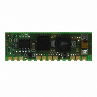
Page 3
... GS-R24FP 1 Pin settings 1.1 Pin connection and mechanical data (dimensions in mm) Figure 1. Pin connection GS-R24FVxxx1.8 Figure 2. Pin connection GS-R24FSxxx1.8 Pin settings 3/15 ...
Page 4
... Pin settings 1.2 Pin description Table 2. Pin description Name Input/output 6 Input/output 4/15 Function A logic high level disables the device. When the pin is open, an INH internal pull up disables the device Sync Master/slave synchronization V 3.3 V reference voltage ref Input + DC input voltage Input + DC input voltage ...
Page 5
... GS-R24FP 2 Maximum ratings 2.1 Absolute maximum ratings Table 3. Absolute maximum ratings Symbol V DC input voltage I I Maximum output current out V INH 1 V Sync 2.2 Thermal data Table 4. Thermal data Symbol T Storage temperature range STG T Operating ambient temperature OP Parameter Parameter Maximum ratings ...
Page 6
... Maximum ratings 2.3 Thermal de-rating Table 5. Thermal de-rating for free air condition (all versions) Symbol I Output current o I Output c urrent o I Output current o 6/15 Parameter Test condition ° ° ° ° ° ° ° ° ° ° ° ° ° °C ...
Page 7
... Total stand-by I qst-by quiescent current f Switching frequency s Reference voltage V ref Short circuit current INH INH threshold voltage V Feedback voltage FB Test condition for GS-R24FPyyy1 1 1 ÷ for GS-R24FPyyy1.8 ÷ > 2 inh 1 ÷ ÷ ref i Device ON Device OFF =16 ÷ ÷ 1 Electrical characteristics Min ...
Page 8
... For this reason the switching frequency is also reduced to keep the inductor current within its maximum threshold limit. The frequency depends on the feedback voltage. As the feedback voltage decreases (due to the reduced duty cycle), the switching frequency decrease too. 8/ disable the device. i Figure 6). GS-R24FP ...
Page 9
... An hysteresis of approximately 20 °C avoids that the devices turns ON and OFF continuously. 4.7 Output voltage programming (GS-R24FP0001.8 only) The GS-R24FP0001.8 output voltage is 5.54 V ± reduce this value connect a resistor between pin 10 (FB) and pin 9 (V The resistor must be located very close to the proper pins, to minimize the injected noise (see Figure 4) ...
Page 10
... Time within 5 °C of actual peak temperature (t Ramp down rate Time from 25 °C to peak temperature Figure 3. Soldering 10/ SMAX P Preheat: MIN) S MAX) S MAX GS-R24FP PB free assembly 3 °C / sec max 150 °C 200 °C 60 – 100 sec 217 °C 40 – 70 sec 240 + 0 °C 10 – 20 sec 6 °C / sec 8 minutes max ...
Page 11
... This threshold is typically 30 % higher than the feedback voltage. Figure 4. Output voltage programming 4, 5 Vin GS-RxxFp000z.z Figure 6. Multiple units synchronization 4, 5 Vin GS-RxxFpyyyz.z Figure Rload Rload 8, 9 Vin 6, 7 Additional features and protections Loop compensation Vin GS-RxxFp000z Rload 8, 9 GS-RxxFpyyyz Rload 11/15 ...
Page 12
... Additional features and protections Figure 7. PCB footprint for GS-R24FSxxx1.8 (dimensions in mm) 12/15 GS-R24FP ...
Page 13
... GS-R24FP 6 Ordering scheme Table 8. Ordering information scheme Input voltage Package V = Vertical S = SMD Output voltage 018 = 1.8 V 025 = 2.5 V 033 = 3.3 V 050 = 5.0 V ÷ 000 = 1.235 5.5 V Output current 1.8 = 1.8 A GS- R12 FV Ordering scheme 018 1.8 13/15 ...
Page 14
... Revision history 7 Revision history Table 9. Document revision history Date 13-Oct-2006 27-Feb-2008 14/15 Revision 1 Initial release 2 Added: Section 4.9: Soldering on page 10 GS-R24FP Changes ...
Page 15
... GS-R24FP Information in this document is provided solely in connection with ST products. STMicroelectronics NV and its subsidiaries (“ST”) reserve the right to make changes, corrections, modifications or improvements, to this document, and the products and services described herein at any time, without notice. All ST products are sold pursuant to ST’s terms and conditions of sale. ...