SI84XXISO-KIT Silicon Laboratories Inc, SI84XXISO-KIT Datasheet - Page 6
SI84XXISO-KIT
Manufacturer Part Number
SI84XXISO-KIT
Description
KIT EVAL FOR SI84XXISO
Manufacturer
Silicon Laboratories Inc
Series
ISOpror
Datasheet
1.SI84XXISO-KIT.pdf
(16 pages)
Specifications of SI84XXISO-KIT
Main Purpose
Interface, Digital Isolator
Embedded
No
Utilized Ic / Part
Si8400, Si8421, Si8442, Si8463
Primary Attributes
DC to 150 Mbps Data Transmission
Secondary Attributes
I²C Interface
Minimum Operating Temperature
- 40 C
Supply Voltage (min)
2.7 V
Product
RF Development Tools
Maximum Frequency
1.7 MHz
Supply Voltage (max)
5 V
Maximum Operating Temperature
+ 125 C
Lead Free Status / RoHS Status
Lead free / RoHS Compliant
Lead Free Status / RoHS Status
Lead free / RoHS Compliant, Lead free / RoHS Compliant
Other names
336-1765


Si84xxISO-EVB UG
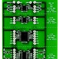
3.1. Digital Isolator Considerations
The Si84xxISO evaluation board (see Figure 1 on page 2) provides a means to evaluate the Si841x,2x,3x,4x,5x,6x
2
digital isolator families as well as the Si8400 isolated I
C family. After power has been supplied to the board,
connect a digital input signal (5 Vpeak max, with desired clock frequency up to 150 Mbps) to the desired input
channel. To view the isolated channel’s data transmission, connect a scope probe to the output channel of interest.
There are various inputs and outputs on either side of the board depending on the device one chooses to evaluate,
as indicated by the silk screen. The board can be used to measure propagation delay, pulse-width distortion,
channel-channel matching, pulse-width skew, and various other parameters.
The nominal output impedance of an isolator driver channel is approximately 50 , ±40%, which is a combination
of the values of the on-chip series termination resistor and the channel resistance of the output driver FET. When
driving loads where transmission line effects will be a factor, output pins should be terminated with 50 controlled
impedance PCB traces.
Figure 5 illustrates the Si8421 transmitting a 500 kHz (5 Vpeak) signal through the Si8421. VDD1 and VDD2 were
powered from 5 V. Channel 1 illustrates the input, and Channel 2 illustrates the output.
Figure 5. 500 kHz (5 V Peak) Signal
6
Rev. 0.3
Related parts for SI84XXISO-KIT
Image
Part Number
Description
Manufacturer
Datasheet
Request
R

Part Number:
Description:
SMD/C°/SINGLE-ENDED OUTPUT SILICON OSCILLATOR
Manufacturer:
Silicon Laboratories Inc
Part Number:
Description:
Manufacturer:
Silicon Laboratories Inc
Datasheet:
Part Number:
Description:
N/A N/A/SI4010 AES KEYFOB DEMO WITH LCD RX
Manufacturer:
Silicon Laboratories Inc
Datasheet:
Part Number:
Description:
N/A N/A/SI4010 SIMPLIFIED KEY FOB DEMO WITH LED RX
Manufacturer:
Silicon Laboratories Inc
Datasheet:
Part Number:
Description:
N/A/-40 TO 85 OC/EZLINK MODULE; F930/4432 HIGH BAND (REV E/B1)
Manufacturer:
Silicon Laboratories Inc
Part Number:
Description:
EZLink Module; F930/4432 Low Band (rev e/B1)
Manufacturer:
Silicon Laboratories Inc
Part Number:
Description:
I°/4460 10 DBM RADIO TEST CARD 434 MHZ
Manufacturer:
Silicon Laboratories Inc
Part Number:
Description:
I°/4461 14 DBM RADIO TEST CARD 868 MHZ
Manufacturer:
Silicon Laboratories Inc
Part Number:
Description:
I°/4463 20 DBM RFSWITCH RADIO TEST CARD 460 MHZ
Manufacturer:
Silicon Laboratories Inc
Part Number:
Description:
I°/4463 20 DBM RADIO TEST CARD 868 MHZ
Manufacturer:
Silicon Laboratories Inc
Part Number:
Description:
I°/4463 27 DBM RADIO TEST CARD 868 MHZ
Manufacturer:
Silicon Laboratories Inc
Part Number:
Description:
I°/4463 SKYWORKS 30 DBM RADIO TEST CARD 915 MHZ
Manufacturer:
Silicon Laboratories Inc
Part Number:
Description:
N/A N/A/-40 TO 85 OC/4463 RFMD 30 DBM RADIO TEST CARD 915 MHZ
Manufacturer:
Silicon Laboratories Inc
Part Number:
Description:
I°/4463 20 DBM RADIO TEST CARD 169 MHZ
Manufacturer:
Silicon Laboratories Inc