MCP3423EV Microchip Technology, MCP3423EV Datasheet - Page 20
MCP3423EV
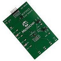
Manufacturer Part Number
MCP3423EV
Description
BOARD EVAL 18BIT 2CH ADC MCP3423
Manufacturer
Microchip Technology
Specifications of MCP3423EV
Number Of Adc's
1
Number Of Bits
18
Sampling Rate (per Second)
3.75
Data Interface
Serial
Inputs Per Adc
2 Differential
Input Range
±VREF
Voltage Supply Source
Single Supply
Operating Temperature
-40°C ~ 125°C
Utilized Ic / Part
MCP3423
Silicon Manufacturer
Microchip
Application Sub Type
ADC
Kit Application Type
Data Converter
Silicon Core Number
MCP3423
Lead Free Status / RoHS Status
Lead free / RoHS Compliant


MCP3422/3/4
FIGURE 5-1:
5.3.2
The MCP3423 and MCP3424 have two external
device address pins (Adr1, Adr0). These pins can be
set to a logic high (or tied to V
or left floating (not connected to anything, or tied to
V
two pins allow eight possible addresses.
shows the device address depending on the logic
status of the address selection pins.
The device samples the logic status of the Adr0 and
Adr1 pins in the following events:
a.
b.
c.
The device samples the logic status (address pins)
during the above events, and latches the values until a
new latch event occurs. During normal operation (after
the address pins are latched), the address pins are
internally disabled from the rests of the internal circuit.
DS22088C-page 20
DD
Note 1:
/2), These combinations of logic level using the
Device power-up.
General Call Reset
(See Section 5.4 “General Call”).
General Call Latch
(See Section 5.4 “General Call”).
Start bit
1
2:
DEVICE ADDRESS BITS (A2, A1, A0)
AND ADDRESS SELECTION PINS
(
Device Code
MCP3423
MCP3423 and MCP3424: Configured by
the user. See
configurations.
MCP3422: Programmed at the factory
during production.
1
0
Address Byte:
Address
Address Byte
Address Byte.
AND
1
Table 5-3
A2
Address Bits
MCP3424
DD
Read/Write bit
), low (or tied to V
A1
Acknowledge bit
for address bit
A0
)
(Note 1)
R/W ACK
Table 5-3
SS
),
It is recommended to issue a General Call Reset or
General Call Latch command once after the device
has powered up. This will ensure that the device reads
the address pins in a stable condition, and avoid
latching the address bits while the power supply is
ramping up. This might cause inaccurate address pin
detection.
When the address pin is left “floating”:
When the address pin is left “floating”, the address pin
momentarily outputs a short pulse with an amplitude of
about V
latches this pin voltage at the same time.
If the “floating” pin is connected to a large parasitic
capacitance (>20 pF) or to a long PCB trace, this short
floating voltage output can be altered. As a result, the
device may not latch the pin correctly.
It is strongly recommended to keep the “floating” pin
pad as short as possible in the customer application
PCB and minimize the parasitic capacitance to the pin
as small as possible (< 20 pF).
Figure 5-2
output at the address pin when the address pin is left
“floating”. The waveform at the Adr0 pin is captured by
using an oscilloscope probe with 15 pF of capacitance.
The device latches the floating condition immediately
after the General Call Latch command.
FIGURE 5-2:
Command and Voltage Output at Address Pin
Left “Floating” (MCP3423 and MCP3424).
Float waveform (output)
at address pin
SDA
SCL
DD
/2 during the latch event. The device also
shows an example of the Latch voltage
General Call Latch
© 2009 Microchip Technology Inc.
Related parts for MCP3423EV
Image
Part Number
Description
Manufacturer
Datasheet
Request
R

Part Number:
Description:
Manufacturer:
Microchip Technology Inc.
Datasheet:
Part Number:
Description:
Manufacturer:
Microchip Technology Inc.
Datasheet:
Part Number:
Description:
Manufacturer:
Microchip Technology Inc.
Datasheet:
Part Number:
Description:
Manufacturer:
Microchip Technology Inc.
Datasheet:
Part Number:
Description:
Manufacturer:
Microchip Technology Inc.
Datasheet:
Part Number:
Description:
Manufacturer:
Microchip Technology Inc.
Datasheet:
Part Number:
Description:
Manufacturer:
Microchip Technology Inc.
Datasheet:
Part Number:
Description:
Manufacturer:
Microchip Technology Inc.
Datasheet: