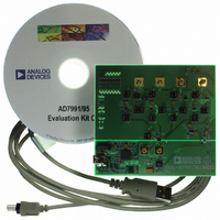
EVAL-AD7991EBZ Analog Devices Inc, EVAL-AD7991EBZ Datasheet - Page 18

EVAL-AD7991EBZ
Manufacturer Part Number
EVAL-AD7991EBZ
Description
BOARD EVAL FOR AD7991
Manufacturer
Analog Devices Inc
Specifications of EVAL-AD7991EBZ
Number Of Adc's
1
Number Of Bits
12
Sampling Rate (per Second)
1M
Data Interface
Serial
Inputs Per Adc
4 Single Ended
Input Range
0 ~ Vdd
Power (typ) @ Conditions
4.4mW @ 5.5 V, 3.4MHz
Voltage Supply Source
Single Supply
Operating Temperature
-40°C ~ 125°C
Utilized Ic / Part
AD7991
Silicon Manufacturer
Analog Devices
Application Sub Type
ADC
Kit Application Type
Data Converter
Silicon Core Number
AD7991
Kit Contents
Board
Rohs Compliant
Yes
Lead Free Status / RoHS Status
Lead free / RoHS Compliant
AD7991/AD7995/AD7999
TYPICAL CONNECTION DIAGRAM
Figure 22 shows the typical connection diagram for the
AD7991/AD7995/AD7999.
The reference voltage can be taken from the supply voltage,
V
to be a 3-channel device with the reference voltage applied to
the V
the V
SDA and SCL form the 2-wire I
pull-up resistors are required for both the SDA and SCL lines.
The AD7991-0/AD7995-0 and the AD7991-1/AD7995-1/
AD7999-1 support standard, fast, and high speed I
modes. Both the -0 and -1 devices have independent I
which allows the devices to connect to the same I
contention issues.
The part requires approximately 0.6 μs to wake up from power-
down and to acquire the analog input. Once the acquisition
phase ends, the conversion phase starts and takes approximately
1 μs to complete. The AD7991/AD7995/AD7999 enters
shutdown mode after each conversion, which is useful in
applications where power consumption is a concern.
DD
. However, the AD7991/AD7995/AD7999 can be configured
IN3
IN3
/V
/V
REF
REF
pin. In this case, a 1 μF decoupling capacitor on
pin is recommended.
2
C compatible interface. External
V
V
V
V
IN0
IN1
IN2
IN3
/V
REF
Figure 22. AD7991/AD7995/AD7999 Typical Connection Diagram
GND
AD7991/
AD7995/
AD7999
2
C bus without
2
2
C interface
C addresses,
V
DD
10µF
SDA
SCL
+
Rev. B | Page 18 of 28
0.1µF
+
R
P
ANALOG INPUT
Figure 21 shows an equivalent circuit of the AD7991/AD7995/
AD7999 analog input structure. The two diodes, D1 and D2,
provide ESD protection for the analog inputs. Care must be taken
to ensure that the analog input signal does not exceed the supply
rails by more than 300 mV. If the signal does exceed this level,
the diodes become forward-biased and start conducting current
into the substrate. Each diode can conduct a maximum current
of 10 mA without causing irreversible damage to the part.
Capacitor C1 in Figure 21 is typically about 4 pF and can
primarily be attributed to pin capacitance. Resistor R1 is a
lumped component composed of the on resistance (R
both a track-and-hold switch and the input multiplexer. The
total resistor is typically about 400 Ω. Capacitor C2, the ADC
sampling capacitor, has a typical capacitance of 30 pF.
R
P
V
IN
4pF
5V SUPPLY
C1
2-WIRE SERIAL
INTERFACE
MICROCONTROLLER/
MICROPROCESSOR
Figure 21. Equivalent Analog Input Circuit
V
DD
D1
D2
CONVERSION PHASE—SWITCH OPEN
TRACK PHASE—SWITCH CLOSED
R1
30pF
C2
ON
) of


