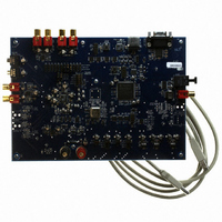
CDB5345 Cirrus Logic Inc, CDB5345 Datasheet
CDB5345
Specifications of CDB5345


Related parts for CDB5345


CDB5345 Summary of contents
Page 1
... CS5345 and other devices operating over a wide range of logic levels. The CS5345 is available in a 48-pin LQFP package in Commercial (-10° to +70° C) and Automotive (-40° to +105° C) grade. The CDB5345 Customer Demonstra- tion board is also available for device evaluation and implementation suggestions. Please refer to Information” on page 41 3 ...
Page 2
TABLE OF CONTENTS 1. PIN DESCRIPTIONS 2. CHARACTERISTICS AND SPECIFICATIONS ...................................................................................... 7 SPECIFIED OPERATING CONDITIONS ............................................................................................. 7 ABSOLUTE MAXIMUM RATINGS ....................................................................................................... 7 ADC ANALOG CHARACTERISTICS ................................................................................................... 8 ADC ANALOG CHARACTERISTICS ................................................................................................. 10 ADC DIGITAL FILTER CHARACTERISTICS ..................................................................................... 11 PGAOUT ANALOG ...
Page 3
Channel B PGA Gain (Bits 5:0) ............................................................................................. 33 6.7 Channel A PGA Control - Address 08h .......................................................................................... 34 6.7.1 Channel A PGA Gain (Bits 5:0) ............................................................................................. 34 6.8 ADC Input Control - Address 09h ................................................................................................... 34 6.8.1 PGA Soft ...
Page 4
Table 5. Freeze-able Bits .......................................................................................................................... 31 Table 6. Functional Mode Selection .......................................................................................................... 32 Table 7. Digital Interface Formats ............................................................................................................. 32 Table 8. MCLK Frequency ........................................................................................................................ 33 Table 9. PGAOut Source Selection ........................................................................................................... 33 Table 10. Example Gain and Attenuation Settings ...
Page 5
PIN DESCRIPTIONS SDA/CDOUT 1 SCL/CCLK 2 AD0/ AD1/CDIN VLC 5 6 RESET 7 AIN3A 8 AIN3B 9 AIN2A 10 AIN2B 11 AIN1A 12 AIN1B Pin Name # Pin Description Serial Control Data (Input/Output) - SDA is a ...
Page 6
AIN1A 11 Stereo Analog Input 1 (Input) - The full-scale level is specified in the ADC Analog Characteristics AIN1B 12 specification table. AGND 13 Analog Ground (Input) - Ground reference for the internal analog section Analog Power (Input) ...
Page 7
CHARACTERISTICS AND SPECIFICATIONS SPECIFIED OPERATING CONDITIONS AGND = DGND = 0 V; All voltages with respect to ground. Parameters DC Power Supplies: Ambient Operating Temperature (Power Applied) Notes: 1. Maximum of VA+0. 5.25 V, whichever is less. ...
Page 8
ADC ANALOG CHARACTERISTICS Test conditions (unless otherwise specified): AGND = DGND = 0.25 V, whichever is less; VLS = VLC = ...
Page 9
Parameter Interchannel Isolation DC Accuracy Gain Error Gain Drift Line-Level Input Characteristics Full-scale Input Voltage Input Impedance Maximum Interchannel Input Impedance Mismatch Parameter DC Accuracy Interchannel Gain Mismatch Programmable Gain Characteristics Gain Step Size Absolute Gain Step Error 4. Valid ...
Page 10
ADC ANALOG CHARACTERISTICS (Continued) Parameter Dynamic Performance for 5.25 V Dynamic Range PGA Setting: - A-weighted unweighted PGA Setting: +12 dB A-weighted unweighted Total Harmonic Distortion + Noise PGA Setting: -12 ...
Page 11
ADC DIGITAL FILTER CHARACTERISTICS Parameter (Notes 8, 10) Single-Speed Mode Passband (-0.1 dB) Passband Ripple Stopband Stopband Attenuation Total Group Delay (Fs = Output Sample Rate) Double-Speed Mode Passband (-0.1 dB) Passband Ripple Stopband Stopband Attenuation Total Group Delay (Fs ...
Page 12
PGAOUT ANALOG CHARACTERISTICS Test conditions (unless otherwise specified): AGND = DGND = 0.25 V, whichever is less; VLS = VLC = ...
Page 13
PGAOUT ANALOG CHARACTERISTICS (Continued) Parameter Dynamic Performance with PGA Line-Level Input Selected Dynamic Range PGA Setting: - A-weighted unweighted PGA Setting: +12 dB Gain A-weighted unweighted Total Harmonic Distortion + Noise PGA Setting: - ...
Page 14
PGAOUT ANALOG CHARACTERISTICS (Continued) Parameter DC Accuracy with PGA Line Level Input Selected Interchannel Gain Mismatch Gain Error Gain Drift DC Accuracy with PGA Mic Level Input Selected Interchannel Gain Mismatch Gain Error Gain Drift Analog Output Frequency Response 10 ...
Page 15
DC ELECTRICAL CHARACTERISTICS AGND = DGND = 0 V, all voltages with respect to ground. MCLK=12.288 MHz; Fs=48 kHz; Master Mode. Parameter Power Supply Current (Normal Operation) Power Supply Current (Power-Down Mode) (Note 13) Power Consumption (Normal Operation) VA, VD, ...
Page 16
DIGITAL INTERFACE CHARACTERISTICS Test conditions (unless otherwise specified): AGND = DGND = 0 V; VLS = VLC = 1. 5.25 V. Parameters (Note 16) High-Level Input Voltage > 2.0 V Low-Level Input Voltage ...
Page 17
SWITCHING CHARACTERISTICS - SERIAL AUDIO PORT Logic ‘0’ = DGND = AGND = 0 V; Logic ‘1’ = VL, C Parameter Sample Rate MCLK Specifications MCLK Frequency MCLK Input Pulse Width High/Low Master Mode LRCK Duty Cycle SCLK Duty Cycle ...
Page 18
LRCK Output SCLK Output SDOUT Figure 1. Master Mode Serial Audio Port Timing LRCK Input SCLK Input SDOUT 18 t slr t sdo t t sclkh slr t sclkw t sdo Figure 2. Slave Mode Serial Audio Port Timing CS5345 ...
Page 19
Channel A - Left LRCK SCLK SDATA MSB - Figure 3. Format 0, Left-Justified up to 24-Bit Data Channel A - Left LRCK SCLK SDATA +5 +4 MSB - DS658F2 ...
Page 20
SWITCHING CHARACTERISTICS - CONTROL PORT - I²C FORMAT Inputs: Logic 0 = DGND = AGND = 0 V, Logic 1 = VLC, C Parameter SCL Clock Frequency RESET Rising Edge to Start Bus Free Time Between Transmissions Start Condition Hold ...
Page 21
SWITCHING CHARACTERISTICS - CONTROL PORT - SPI FORMAT Inputs: Logic 0 = DGND = AGND = 0 V, Logic 1 = VLC, C Parameter CCLK Clock Frequency RESET Rising Edge to CS Falling CS High Time Between Transmissions CS Falling ...
Page 22
TYPICAL CONNECTION DIAGRAM +3.3V to +5V 10 µF +1.8V to +5V 0.1 µF Digital Audio Capture Micro- Controller 2 kΩ 2 kΩ See Note 1 +1.8V to +5V 0.1 µF Note 1: Resistors are required for I²C control port ...
Page 23
APPLICATIONS 4.1 Recommended Power-Up Sequence 1. Hold RESET low until the power supply,MCLK, and LRCK are stable. In this state, the Control Port is reset to its default settings. 2. Bring RESET high. The device will remain in a ...
Page 24
Master Mode As a clock master, LRCK and SCLK will operate as outputs. LRCK and SCLK are internally derived from MCLK with LRCK equal to Fs and SCLK equal shown in MCLK 4.2.3 Slave ...
Page 25
Analog Input Multiplexer, PGA, and Mic Gain The CS5345 contains a stereo 6-to-1 analog input multiplexer followed by a programmable gain amplifier (PGA). The input multiplexer can select one of six possible stereo analog input sources and route it ...
Page 26
Control Port Description and Timing The control port is used to access the registers, allowing the CS5345 to be configured for the desired oper- ational modes and formats. The operation of the control port may be completely asynchronous with ...
Page 27
VLC or DGND as desired. The state of the pins is sensed while the CS5345 is being reset. The signal timings for a read and write cycle are shown in defined as a falling ...
Page 28
Receive byte, contents of selected register. Send acknowledge bit. Send stop condition. 4.8 Interrupts and Overflow The CS5345 has a comprehensive interrupt capability. The INT output pin is intended to drive the interrupt input pin on the host microcontroller. The ...
Page 29
VLC) or may be powered from the analog supply (VA) via a resistor. In this case, no additional devices should be powered from VD. Power supply decoupling capacitors should be as near to the CS5345 ...
Page 30
REGISTER QUICK REFERENCE This table shows the register names and their associated default values. Addr Function 7 01h Chip ID PART3 PART2 1 02h Power Control Freeze Reserved Reserved Reserved 0 03h Reserved Reserved Reserved Reserved Reserved 0 04h ...
Page 31
REGISTER DESCRIPTION 6.1 Chip ID - Register 01h 7 6 PART3 PART2 PART1 Function: This register is Read-Only. Bits 7 through 4 are the part number ID, which is 1110b (0Eh), and the remaining bits (3 through 0) indicate ...
Page 32
ADC Control - Address 04h 7 6 FM1 FM0 Reserved 6.3.1 Functional Mode (Bits 7:6) Function: Selects the required range of sample rates. FM1 FM0 6.3.2 Digital Interface Format (Bit 4) ...
Page 33
MCLK Frequency - Address 05h 7 6 MCLK MCLK Reserved Freq2 Freq1 6.4.1 Master Clock Dividers (Bits 6:4) Function: Sets the frequency of the supplied MCLK signal. See MCLK Divider ÷ 1 ÷ 1.5 ÷ 2 ÷ 3 ÷ ...
Page 34
Channel A PGA Control - Address 08h 7 6 Reserved Reserved Gain5 6.7.1 Channel A PGA Gain (Bits 5:0) Function: Sets the gain or attenuation for the ADC input PGA stage. The gain may be adjusted from -12 dB ...
Page 35
PGASoft PGAZeroCross Table 11. PGA Soft Cross or Zero Cross Mode Selection 6.8.2 Analog Input Selection (Bits 2:0) Function: These bits are used to select the input source for the PGA and ADC. Please see Sel2 ...
Page 36
Clock Error (Bit 3) Function: Indicates the occurrence of a clock error condition. 6.10.2 Overflow (Bit 1) Function: Indicates the occurrence of an ADC overflow condition. 6.10.3 Underflow (Bit 0) Function: Indicates the occurrence of an ADC underflow condition. ...
Page 37
PARAMETER DEFINITIONS Dynamic Range The ratio of the rms value of the signal to the rms sum of all other spectral components over the specified bandwidth. Dynamic Range is a signal-to-noise ratio measurement over the specified bandwidth made with ...
Page 38
FILTER PLOTS 0 -10 -20 -30 -40 -50 -60 -70 -80 -90 -100 -110 -120 -130 -140 0.0 0.1 0.2 0.3 0.4 0.5 Frequency (norm alized to Fs) Figure 13. Single-Speed Stopband Rejection ...
Page 39
Frequency (norm alized to Fs) Figure 19. Double-Speed Transition Band (Detail) 0 -10 -20 -30 -40 -50 -60 -70 -80 -90 -100 -110 -120 -130 ...
Page 40
PACKAGE DIMENSIONS 48L LQFP PACKAGE DRAWING D D1 DIM MIN A --- A1 0.002 B 0.007 D 0.343 D1 0.272 E 0.343 E1 0.272 e* 0.016 L 0.018 ∝ 0.000° * Nominal pin pitch is 0.50 mm 10.THERMAL CHARACTERISTICS ...
Page 41
... CS5345 Container Order # Tray CS5345-CQZ Tape & Reel CS5345-CQZR Tray CS5345-DQZ Tape & Reel CS5345-DQZR - - CDB5345 Control Port Description and Timing description on page 31. 5. page 17. table on page 21. Channel A PGA Control - Address 08h section on 41 ...