CDB5529 Cirrus Logic Inc, CDB5529 Datasheet - Page 7
CDB5529
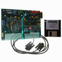
Manufacturer Part Number
CDB5529
Description
EVAL BOARD FOR CS5529
Manufacturer
Cirrus Logic Inc
Specifications of CDB5529
Number Of Adc's
1
Number Of Bits
16
Sampling Rate (per Second)
303
Data Interface
Serial
Inputs Per Adc
2 Differential
Input Range
±2.5 V
Power (typ) @ Conditions
2.6mW @ 2.5 V
Voltage Supply Source
Analog and Digital, Dual ±
Operating Temperature
-40°C ~ 85°C
Utilized Ic / Part
CS5529
Lead Free Status / RoHS Status
Contains lead / RoHS non-compliant
Other names
598-1015


ABSOLUTE MAXIMUM RATINGS
Notes: 13. All voltages with respect to ground.
WARNING: Operation at or beyond these limits may result in permanent damage to the device.
DS246F5
DC Power Supplies
Input Current, Any Pin Except Supplies
Output Current
Power Dissipation
Analog Input Voltage
Digital Input Voltage
Ambient Operating Temperature
Storage Temperature
14. VA+ and VA- must satisfy {(VA+) - (VA-)} ≤ +6.3 V; and |VA-| must be ≤ VA+.
15. VD+ and VA- must satisfy {(VD+) - (VA-)} ≤ +7.75 V.
16. Applies to all pins including continuous overvoltage conditions at the analog input (AIN) pins.
17. Transient current of up to 100mA will not cause SCR latch-up. Maximum input current for a power
18. Total power dissipation, including all input currents and output currents.
supply pin is ±50 mA.
Normal operation is not guaranteed at these extremes.
Parameter
AIN and VREF pins
(Notes 14 and 15)
(Notes 16 and 17)
Negative Analog
Positive Analog
Positive Digital
(DGND = 0 V) (See Note 13.)
(Note 18)
Symbol
PDN
VD+
I
V
V
VA+
VA-
T
OUT
I
T
INA
IND
IN
stg
A
(VA-) + (-0.3)
Min
-0.3
-0.3
-6.0
-0.3
-40
-65
-
-
-
Typ
-
-
-
-
-
-
-
-
-
-
(VD+)+0.3
(VA+)+0.3
+150
Max
+6.0
+6.0
+0.3
+85
±10
±25
8
CS5529
Unit
mW
mA
mA
°C
°C
V
V
V
V
V
7
Related parts for CDB5529
Image
Part Number
Description
Manufacturer
Datasheet
Request
R

Part Number:
Description:
Development Kit
Manufacturer:
Cirrus Logic Inc
Datasheet:
Part Number:
Description:
Development Kit
Manufacturer:
Cirrus Logic Inc
Datasheet:


Part Number:
Description:
High-efficiency PFC + Fluorescent Lamp Driver Reference Design
Manufacturer:
Cirrus Logic Inc
Datasheet:
Part Number:
Description:
Development Kit
Manufacturer:
Cirrus Logic Inc
Datasheet:
Part Number:
Description:
Development Kit
Manufacturer:
Cirrus Logic Inc
Datasheet:

Part Number:
Description:
Development Kit
Manufacturer:
Cirrus Logic Inc
Datasheet:
Part Number:
Description:
Development Kit
Manufacturer:
Cirrus Logic Inc
Datasheet:
Part Number:
Description:
Development Kit
Manufacturer:
Cirrus Logic Inc
Datasheet:
Part Number:
Description:
Development Kit
Manufacturer:
Cirrus Logic Inc
Datasheet:

Part Number:
Description:
EVALUATION BOARD FOR CS8427
Manufacturer:
Cirrus Logic Inc
Datasheet:

Part Number:
Description:
BOARD EVAL FOR CS8416 RCVR
Manufacturer:
Cirrus Logic Inc
Datasheet:

Part Number:
Description:
EVALUATION BOARD FOR CS8420
Manufacturer:
Cirrus Logic Inc
Datasheet:

Part Number:
Description:
KIT DEVELOPMENT EP9315 ARM9
Manufacturer:
Cirrus Logic Inc
Datasheet:

Part Number:
Description:
KIT DEVELOPMENT EP9302 ARM9
Manufacturer:
Cirrus Logic Inc
Datasheet: