MCP1630DM-DDBS1 Microchip Technology, MCP1630DM-DDBS1 Datasheet - Page 11
MCP1630DM-DDBS1
Manufacturer Part Number
MCP1630DM-DDBS1
Description
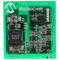
BOARD DEMO BOOST AUTO INPUT
Manufacturer
Microchip Technology
Type
DC/DC Switching Converters, Regulators & Controllersr
Specifications of MCP1630DM-DDBS1
Main Purpose
DC/DC, Step Up
Outputs And Type
1, Non-Isolated
Voltage - Output
36.5V
Current - Output
400mA
Voltage - Input
9 ~ 18V
Regulator Topology
Boost
Frequency - Switching
500kHz
Board Type
Fully Populated
Utilized Ic / Part
MCP1630
Silicon Manufacturer
Microchip
Silicon Core Number
MCP1630, PIC12F683
Core Architecture
PIC
Core Sub-architecture
PIC12
Silicon Family Name
Piccolo
Product
Power Management Modules
Lead Free Status / RoHS Status
Not applicable / Not applicable
Power - Output
-
Lead Free Status / Rohs Status
Lead free / RoHS Compliant
For Use With/related Products
MCP1630, PIC12F683
Lead Free Status / RoHS Status
Lead free / RoHS Compliant, Not applicable / Not applicable


3.0
The descriptions of the pins are listed in Table 3-1.
TABLE 3-1:
3.1
COMP is an internal error amplifier output pin. External
compensation is connected from the FB pin to the
COMP pin for control-loop stabilization. An internal
voltage clamp is used to limit the maximum COMP pin
voltage to 2.7V (typ.). This clamp is used to set the
maximum peak current in the power system switch by
setting a maximum limit on the CS input for Peak
Current mode control systems.
3.2
FB is an internal error amplifier inverting input pin. The
output (voltage or current) is sensed and fed back to
the FB pin for regulation. Inverting or negative
feedback is used.
3.3
CS is the current sense input pin used for cycle-by-
cycle control for Peak Current mode converters. The
MCP1630 is typically used for sensed current
applications to reduce the current sense signal, thus
reducing power dissipation.
For
applications, a ramp is used to compare the error
amplifier output voltage with producing the PWM duty
cycle. For applications that require higher signal levels,
the MCP1630V is used to increase the level from a
maximum of 0.9V (MCP1630) to 2.7V (MCP1630V).
The common mode voltage range for the MCP1630V
CS input is V
CS input should be less than or equal to V
all times.
3.4
OSC is an external oscillator input pin. Typically, a
microcontroller I/O pin is used to generate the OSC
input. When high, the output driver pin (V
© 2005 Microchip Technology Inc.
DFN/MSOP
Voltage mode or
1
2
3
4
5
6
7
8
MCP1630 PIN DESCRIPTIONS
Error Amplifier Output Pin (COMP)
Error Amplifier Inverting Input
(FB)
Current Sensing Input (CS)
Oscillator Input (OSC)
IN
-1.4V. For normal PWM operation, the
OSC IN
COMP
Name
GND
V
V
PIN FUNCTION TABLE
CS
V
FB
EXT
REF
IN
Error Amplifier Output pin
Error Amplifier Inverting Input
Current Sense Input pin (MCP1630) or Voltage Ramp Input pin (MCP1630V)
Oscillator Input pin
Circuit Ground pin
External Driver Output pin
Input Bias pin
Reference Voltage Input pin
Average
Current
EXT
IN
) is driven
- 1.4V at
mode
MCP1630/MCP1630V
low. The high-to-low transition initiates the start of a
new cycle. The duty cycle of the OSC input pin deter-
mines the maximum duty cycle of the power converter.
For example, if the OSC input is low for 75% of the time
and high for 25% of the time, the duty cycle range for
the power converter is 0% to 75% maximum.
3.5
Connect the circuit ground to the GND pin. For most
applications, this should be connected to the analog or
quiet ground plane. Noise on this ground can affect the
sensitive cycle-by-cycle comparison between the CS
input and the error amplifier output.
3.6
V
the power system duty cycle. For high-power or high-
side drives, this output should be connected to the logic-
level input of the MOSFET driver. For low-power, low-
side applications, the V
drive the gate of an N-channel MOSFET.
3.7
V
source to the V
on the V
0.1 µF bypass capacitor should be connected between
the V
3.8
V
the output of the power system. By changing the V
input, the output (voltage or current) of the power sys-
tem can be changed. The reference voltage can range
from 0V to V
EXT
IN
REF
is an input voltage pin. Connect the input voltage
Function
IN
is an external driver output pin, used to determine
is an external reference input pin used to regulate
pin and the GND pin.
IN
Ground (GND)
External Driver Output Pin (V
Input Bias Pin (V
Reference Voltage Input (V
pin should be between +3.0V and +5.5V. A
IN
IN
(rail-to-rail).
pin. For normal operation, the voltage
EXT
pin can be used to directly
IN
)
DS21896B-page 11
REF
EXT
)
REF
)
Related parts for MCP1630DM-DDBS1
Image
Part Number
Description
Manufacturer
Datasheet
Request
R

Part Number:
Description:
BOARD CONV DEMO MCP1630 TRPL-OUT
Manufacturer:
Microchip Technology
Datasheet:

Part Number:
Description:
BOARD DEMO FOR MCP1630
Manufacturer:
Microchip Technology
Datasheet:

Part Number:
Description:
BOARD DEMO MCP1630 BIAS SUPPLY
Manufacturer:
Microchip Technology
Datasheet:

Part Number:
Description:
BOARD DEMO BOOST COUPLED INDUCTR
Manufacturer:
Microchip Technology
Datasheet:

Part Number:
Description:
BOARD DEM MCP1630 BOOST MODE LED
Manufacturer:
Microchip Technology
Datasheet:

Part Number:
Description:
Manufacturer:
Microchip Technology Inc.
Datasheet:
Part Number:
Description:
Manufacturer:
Microchip Technology Inc.
Datasheet:
Part Number:
Description:
Manufacturer:
Microchip Technology Inc.
Datasheet:
Part Number:
Description:
Manufacturer:
Microchip Technology Inc.
Datasheet:
Part Number:
Description:
Manufacturer:
Microchip Technology Inc.
Datasheet:
Part Number:
Description:
Manufacturer:
Microchip Technology Inc.
Datasheet: