NCP1521UEVB ON Semiconductor, NCP1521UEVB Datasheet - Page 3
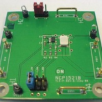
NCP1521UEVB
Manufacturer Part Number
NCP1521UEVB
Description
EVAL BOARD FOR NCP1521U
Manufacturer
ON Semiconductor
Specifications of NCP1521UEVB
Design Resources
NCP1521UEVB BOM NCP1521UEVB Schematic NCP1521UEVB Gerber Files
Main Purpose
DC/DC, Step Down
Outputs And Type
1, Non-Isolated
Voltage - Output
0.9 ~ 3.3 V
Current - Output
600mA
Voltage - Input
3.6V
Regulator Topology
Buck
Frequency - Switching
1.5MHz
Board Type
Fully Populated
Utilized Ic / Part
NCP1521
Lead Free Status / RoHS Status
Lead free / RoHS Compliant
Power - Output
-
Lead Free Status / Rohs Status
Lead free / RoHS Compliant
For Use With/related Products
NCP1521U
Other names
NCP1521UEVBOS


Stresses exceeding Maximum Ratings may damage the device. Maximum Ratings are stress ratings only. Functional operation above the
Recommended Operating Conditions is not implied. Extended exposure to stresses above the Recommended Operating Conditions may affect
device reliability.
1. Maximum electrical ratings are defined as those values beyond which damage to the device may occur at T
2. According to JEDEC standard JESD22-A108B.
3. This device series contains ESD protection and exceeds the following tests:
4. Latchup current maximum rating per JEDEC standard: JESD78.
PIN FUNCTION DESCRIPTION
MAXIMUM RATINGS
Pin No.
Minimum Voltage All Pins
Maximum Voltage All Pins (Note 2)
Maximum Voltage Enable, FB, LX
Thermal Resistance, Junction -to-Air
Operating Ambient Temperature Range
Storage Temperature Range
Junction Operating Temperature
Latch-up Current Maximum Rating (T
ESD Withstand Voltage (Note 3)
Human Body Model
Machine Model
Human Body Model (HBM) per JEDEC standard: JESD22-A114.
Machine Model (MM) per JEDEC standard: JESD22-A115.
1
2
3
4
5
Symbol
GND
VIN
EN
FB
LX
Analog Output
Analog/Power
Analog Input
Analog Input
Digital Input
Function
Ground
Rating
A
= 85°C) (Note 4)
Power Supply Input for Analog V
Ground connection for the NFET Power Stage and the Analog Sections of the IC.
Enable for Switching Regulator. This pin is active high. Do not float this pin.
Feedback voltage from the output of the power supply. This is the input to the error
amplifier.
Connection from Power MOSFETs to the Inductor. For one option, an output discharge
circuit sinks current from this pin.
Figure 4. Pin Connections
GND
VIN
PIN CONNECTIONS
EN
http://onsemi.com
1
2
3
NCP1521
(Top View)
3
5
4
LX
FB
CC
.
Symbol
Description
V
V
Vesd
R
V
T
T
Lu
max
max
T
min
qJA
stg
A
j
-55 to 150
-40 to 125
VIN + 0.3
-40 to 85
A
+/-100
Value
-0.3
= 25°C.
300
200
7.0
2.0
_C/W
Unit
mA
_C
_C
_C
kV
V
V
V
V
Related parts for NCP1521UEVB
Image
Part Number
Description
Manufacturer
Datasheet
Request
R

Part Number:
Description:
1.5 Mhz, 600 Ma, Highefficiency, Low Quiescent Current, Adjustable Output Voltage Stepdown Converter
Manufacturer:
ON Semiconductor
Datasheet:
Part Number:
Description:
ON Semiconductor [VOLTAGE REGULATOR]
Manufacturer:
ON Semiconductor
Datasheet:
Part Number:
Description:
357-036-542-201 CARDEDGE 36POS DL .156 BLK LOPRO
Manufacturer:
ON Semiconductor
Datasheet:
Part Number:
Description:
357-036-542-201 CARDEDGE 36POS DL .156 BLK LOPRO
Manufacturer:
ON Semiconductor
Datasheet:
Part Number:
Description:
357-036-542-201 CARDEDGE 36POS DL .156 BLK LOPRO
Manufacturer:
ON Semiconductor
Datasheet:
Part Number:
Description:
357-036-542-201 CARDEDGE 36POS DL .156 BLK LOPRO
Manufacturer:
ON Semiconductor
Datasheet:
Part Number:
Description:
357-036-542-201 CARDEDGE 36POS DL .156 BLK LOPRO
Manufacturer:
ON Semiconductor
Datasheet:
Part Number:
Description:
357-036-542-201 CARDEDGE 36POS DL .156 BLK LOPRO
Manufacturer:
ON Semiconductor
Datasheet:
Part Number:
Description:
357-036-542-201 CARDEDGE 36POS DL .156 BLK LOPRO
Manufacturer:
ON Semiconductor
Datasheet:
Part Number:
Description:
357-036-542-201 CARDEDGE 36POS DL .156 BLK LOPRO
Manufacturer:
ON Semiconductor
Datasheet:
Part Number:
Description:
357-036-542-201 CARDEDGE 36POS DL .156 BLK LOPRO
Manufacturer:
ON Semiconductor
Datasheet:
Part Number:
Description:
357-036-542-201 CARDEDGE 36POS DL .156 BLK LOPRO
Manufacturer:
ON Semiconductor
Datasheet:
Part Number:
Description:
Manufacturer:
ON Semiconductor
Datasheet:
Part Number:
Description:
Manufacturer:
ON Semiconductor
Datasheet: