MCP4725EV Microchip Technology, MCP4725EV Datasheet - Page 21
MCP4725EV
Manufacturer Part Number
MCP4725EV
Description
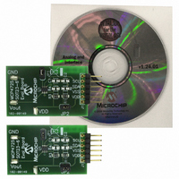
BOARD EVAL FOR MCP4725
Manufacturer
Microchip Technology
Datasheets
1.MCP4725A1T-ECH.pdf
(50 pages)
2.MCP4725EV.pdf
(32 pages)
3.MCP4725A0T-ECH.pdf
(42 pages)
Specifications of MCP4725EV
Number Of Dac's
1
Number Of Bits
12
Outputs And Type
1, Single Ended
Sampling Rate (per Second)
100k ~ 3.4M
Data Interface
I²C
Settling Time
6µs
Dac Type
Voltage
Voltage Supply Source
Single
Operating Temperature
-40°C ~ 125°C
Utilized Ic / Part
MCP4725
Processor To Be Evaluated
MCP4725
Lead Free Status / RoHS Status
Lead free / RoHS Compliant


7.0
7.1
The MCP4725 device uses a two-wire I
interface that can operate on a standard, fast or high
speed mode. A device that sends data onto the bus is
defined as transmitter, and a device receiving data as
receiver. The bus has to be controlled by a master
device which generates the serial clock (SCL), controls
the bus access and generates the START and STOP
conditions. The MCP4725 device works as slave. Both
master and slave can operate as transmitter or
receiver, but the master device determines which mode
is activated. An example of hardware connection
diagram is shown in
initiated by the master (microcontroller) which sends
the START bit, followed by the slave address byte. The
first byte transmitted is always the slave address byte,
which contains the device code, the address bits, and
the R/W bit. The device code for the MCP4725 device
is 1100.
When the device receives a read command (R/W = 1),
it transmits the contents of the DAC input register and
EEPROM. A non-acknowledge (NAK) or repeated start
bit can be transmitted at any time. See
the read operation example. If writing to the device (R/
W = 0), the device will expect write command type bits
in the following byte. See
the write operation examples.
The MCP4725 supports all three I
• Standard Mode: bit rates up to 100 kbit/s
• Fast Mode: bit rates up to 400 kbit/s
• High Speed Mode (HS mode): bit rates up to
Refer to the Phillips I
the I
© 2007 Microchip Technology Inc.
3.4 Mbit/s
2
C specifications.
I
COMMUNICATION
OVERVIEW
2
C SERIAL INTERFACE
2
C document for more details of
Figure
Figure 6-1
8-1. Communication is
2
C operating modes:
and
Figure 6-3
Figure 6-2
2
C serial
for
for
7.2
The address byte is the first byte received following the
START condition from the master device. The first part
of the address byte consists of a 4-bit device code
which is set to 1100 for the MCP4725. The device code
is followed by three address bits (A2, A1, A0) which are
programmed as follows:
• The choice of A2 and A1 bits are provided by the
• The A2 and A1 are programmed to ‘00’ (default),
• A0 bit is determined by the logic state of A0 pin.
When the device receives an address byte, it compares
the logic state of the A0 pin with the A0 address bit
received before responding with the acknowledge bit.
The logic state of the A0 pin needs to be set prior to the
interface communication.
FIGURE 7-1:
Note: A2 and A1: Programmed (hard-wired) at the factory.
customer as part of the ordering process. These
bits are then programmed (hard-wired) during
manufacturing
if not requested by customer
The A0 pin can be tied to V
actively driven by digital logic levels. The advan-
tage of using the A0 pin is that the users can con-
trol the A0 bit on their application PCB circuit and
also two identical MCP4725 devices can be used
on the same bus line.
Start bit
Please Contact Microchip Technology Inc. for A2 and
A1 programming options.
A0: Use the logic level state of A0 pin.
Device Addressing
1
Device Code
Slave Address for MCP4725
1
Slave Address
0
Address Byte
Device Addressing
Read/Write bit
0
DD
MCP4725
Acknowledge bit
A2
or V
Address Bits
DS22039C-page 21
SS
A1
, or can be
A0
R/W
ACK
Related parts for MCP4725EV
Image
Part Number
Description
Manufacturer
Datasheet
Request
R

Part Number:
Description:
Manufacturer:
Microchip Technology Inc.
Datasheet:
Part Number:
Description:
Manufacturer:
Microchip Technology Inc.
Datasheet:
Part Number:
Description:
Manufacturer:
Microchip Technology Inc.
Datasheet:
Part Number:
Description:
Manufacturer:
Microchip Technology Inc.
Datasheet:
Part Number:
Description:
Manufacturer:
Microchip Technology Inc.
Datasheet:
Part Number:
Description:
Manufacturer:
Microchip Technology Inc.
Datasheet:
Part Number:
Description:
Manufacturer:
Microchip Technology Inc.
Datasheet:
Part Number:
Description:
Manufacturer:
Microchip Technology Inc.
Datasheet: