AD9117-EBZ Analog Devices Inc, AD9117-EBZ Datasheet
AD9117-EBZ
Specifications of AD9117-EBZ


Related parts for AD9117-EBZ


AD9117-EBZ Summary of contents
Page 1
... Sleep mode: < 3.3 V Supply voltage: 1 3.3 V SFDR to Nyquist 86 dBc @ 1 MHz output 85 dBc @ 10 MHz output AD9117 NSD @ 1 MHz output, 125 MSPS, 20 mA: −162 dBc/Hz Differential current outputs on-chip auxiliary DACs CMOS inputs with single-port operation Output common mode: adjustable 1.2 V Small footprint 40-lead LFCSP RoHS-compliant package ...
Page 2
... AD9114/AD9115/AD9116/AD9117 TABLE OF CONTENTS Features .............................................................................................. 1 Applications ....................................................................................... 1 General Description ......................................................................... 1 Product Highlights ........................................................................... 1 Revision History ............................................................................... 3 Functional Block Diagram .............................................................. 4 Specifications ..................................................................................... 5 DC Specifications ......................................................................... 5 Digital Specifications ................................................................... 7 AC Specifications .......................................................................... 8 Absolute Maximum Ratings ............................................................ 9 Thermal Resistance ...................................................................... 9 ESD Caution .................................................................................. 9 Pin Configurations and Function Descriptions ......................... 10 Typical Performance Characteristics ........................................... 18 Terminology .................................................................................... 31 Theory of Operation ...................................................................... 32 Serial Peripheral Interface (SPI) ................................................... 33 General Operation of the Serial Interface ...
Page 3
... Changes to Typical Performance Characteristics Section ......... 18 Changes to Theory of Operation Section and Figure 84 ........... 32 Added Figure 85 to Figure 88; Renumbered Sequentially ......... 34 Changes to Table 13 ........................................................................ 35 AD9114/AD9115/AD9116/AD9117 Changes to Table 14 ........................................................................ 36 Changes to Digital Interface Operation Section and Figure 89, Figure 90, Figure 91, Figure 92, and Figure 93 ............................ 40 Changes to Figure 94, Digital Data Latching Section, and Retimer Section ...
Page 4
... I REF 100µA BAND AUX1DAC GAP 1 INTO 2 INTERLEAVED AUX2DAC I DATA DATA INTERFACE Q DATA CLOCK DIST Figure 1. Rev Page AD9117 IR SET 2kΩ 60Ω TO RLIN 260Ω 62.5Ω IOUTN I DAC IOUTP 62.5Ω RLIP AVDD AVSS RLQP 62.5Ω ...
Page 5
... V − 0. Rev Page AD9114/AD9115/AD9116/AD9117 = 20 mA, maximum sample rate, unless otherwise noted. AD9116 AD9117 Min Typ Max Min Typ 12 14 ±0.4 ±1.4 ±0.2 ±0.6 ±0.68 ±1.2 ±0.42 ±0.6 ±0.5 ±1.8 ±0.2 ±1.0 ±0.5 ±1.8 ±0.3 ±1.1 −1 +1 −1 −2 +2 − ...
Page 6
... Rev Page AD9116 AD9117 Min Typ Max Min Typ Max 0.98 1.025 1.08 0.98 1.025 1. 0.1 1.25 0.1 1.25 0.1 1.0 0.1 1 −1 +1 −1 +1 1.7 3.5 1.7 3.5 1.7 3.5 1 ...
Page 7
... V Q Channel or DCLKIO Falling Edge Setup Hold 1 Channel or DCLKIO Rising Edge Setup Hold 3 Channel or DCLKIO Falling Edge Setup Hold 3 Channel or DCLKIO Rising Edge Setup Hold AD9114/AD9115/AD9116/AD9117 = 20 mA, maximum sample rate, unless otherwise noted. xOUTFS Min 2.1 2.1 Rev Page Typ Max Unit 0.9 V 125 ...
Page 8
... AD9116 AD9117 Min Typ Max Min Typ −153 −157 −146 −149 −78 −78 −80 − mA, maximum sample rate, unless otherwise noted. AD9116 AD9117 Min Typ Max Min Typ −146 −150 −135 −138 −69 −69 −72 −72 Max Unit dBc dBc ...
Page 9
... AD9114, 9 for the AD9115, 11 for the AD9116, and 13 for the AD9117. Stresses above those listed under Absolute Maximum Ratings may cause permanent damage to the device. This is a stress rating only; functional operation of the device at these or any other conditions above those indicated in the operational section of this specification is not implied ...
Page 10
... AD9114/AD9115/AD9116/AD9117 PIN CONFIGURATIONS AND FUNCTION DESCRIPTIONS Table 7. AD9114 Pin Function Descriptions Pin No. Mnemonic Description DB[5:2] Digital Inputs. 5 DVDDIO Digital I/O Supply Voltage Input (1 3.3 V Nominal). 6 DVSS Digital Common. 7 DVDD Digital Core Supply Voltage Output (1.8 V). Strap DVDD to DVDDIO at 1 DVDDIO > 1.8 V, bypass DVDD with a 1.0 μ ...
Page 11
... The exposed pad is connected to AVSS and must be soldered to the ground plane. Exposed metal at the package corners is connected to this pad. resistor recommended to leave this pin unconnected. When the internal on-chip (IR Rev Page AD9114/AD9115/AD9116/AD9117 ) is enabled, this pin is connected to the CML ) is disabled, this pin is the full-scale SET ) is enabled, this pin is the auxiliary Q DAC output ...
Page 12
... AD9114/AD9115/AD9116/AD9117 Table 8. AD9115 Pin Function Description Pin No. Mnemonic Description DB[7:4] Digital Inputs. 5 DVDDIO Digital I/O Supply Voltage Input (1 3.3 V Nominal). 6 DVSS Digital Common. 7 DVDD Digital Core Supply Voltage Output (1.8 V). Strap DVDD to DVDDIO at 1 DVDDIO > 1.8 V, bypass DVDD with a 1.0 μF capacitor; however, do not otherwise connect it. The LDO should not drive external loads. ...
Page 13
... The exposed pad is connected to AVSS and must be soldered to the ground plane. Exposed metal at the package corners is connected to this pad. resistor recommended to leave this pin unconnected. When the internal on-chip (IR Rev Page AD9114/AD9115/AD9116/AD9117 ) is enabled, this pin is connected to the CML ) is disabled, this pin is the full- SET ) is enabled, this pin is the auxiliary Q DAC output ...
Page 14
... AD9114/AD9115/AD9116/AD9117 Table 9. AD9116 Pin Function Descriptions Pin No. Mnemonic Description DB[9:6] Digital Inputs. 5 DVDDIO Digital I/O Supply Voltage Input (1 3.3 V Nominal). 6 DVSS Digital Common. 7 DVDD Digital Core Supply Voltage Output (1.8 V). Strap DVDD to DVDDIO at 1 DVDDIO > 1.8 V, bypass DVDD with a 1.0 μF capacitor; however, do not otherwise connect it. The LDO should not drive external loads. ...
Page 15
... The exposed pad is connected to AVSS and must be soldered to the ground plane. Exposed metal at the package corners is connected to this pad. resistor recommended to leave this pin unconnected. When the internal on-chip (IR CML Rev Page AD9114/AD9115/AD9116/AD9117 ) is enabled, this pin is connected to the CML ) is disabled, this pin is the full- SET ) is enabled, this pin is the auxiliary Q DAC output ...
Page 16
... AD9114/AD9115/AD9116/AD9117 Table 10. AD9117 Pin Function Descriptions Pin No. Mnemonic Description DB[11:8] Digital Inputs. 5 DVDDIO Digital I/O Supply Voltage Input (1 3.3 V Nominal). 6 DVSS Digital Common. 7 DVDD Digital Core Supply Voltage Output (1.8 V). Strap DVDD to DVDDIO at 1 DVDDIO > 1.8 V, bypass DVDD with a 1.0 μF capacitor; however, do not otherwise connect it. The LDO should not drive external loads. ...
Page 17
... The exposed pad is connected to AVSS and must be soldered to the ground plane. Exposed metal at the package corners is connected to this pad. resistor recommended to leave this pin unconnected. When the internal on-chip (IR CML Rev Page AD9114/AD9115/AD9116/AD9117 ) is enabled, this pin is connected to CML ) is disabled, this pin is the full- SET ) is enabled, this pin is the auxiliary Q DAC output ...
Page 18
... Figure 9. AD9117 Postcalibration INL at 1 (DVDD = 1.8 V) 2.0 1.5 1.0 0.5 0 –0.5 –1.0 –1.5 –2.0 0 Figure 10. AD9117 Postcalibration DNL at 1 (DVDD = 1.8 V) 1.5 1.0 0.5 0 –0.5 –1.0 –1.5 0 Figure 11. AD9117 Postcalibration INL at 3 (DVDD = 1.8 V) Rev Page 2048 4096 6144 ...
Page 19
... CODE Figure 12. AD9117 Precalibration DNL at 3 0.8 0.6 0.4 0.2 0 –0.2 –0.4 –0.6 –0.8 0 512 1024 1536 2048 2560 3072 CODE Figure 13. AD9116 Precalibration INL at 1 0.6 ...
Page 20
... AD9114/AD9115/AD9116/AD9117 0.8 0.6 0.4 0.2 0 –0.2 –0.4 –0.6 –0.8 0 512 1024 1536 2048 2560 CODE Figure 18. AD9116 Precalibration INL at 3 0.5 0.4 0.3 0.2 0.1 0 –0.1 –0.2 –0.3 –0.4 –0.5 0 512 1024 1536 2048 2560 CODE Figure 19. AD9116 Precalibration DNL at 3 0.25 ...
Page 21
... CODE Figure 26. AD9115 Precalibration DNL at 3 AD9114/AD9115/AD9116/AD9117 0.08 0.06 0.04 0.02 0 –0.02 –0.04 –0.06 –0.08 896 1024 0 128 Figure 27. AD9115 Postcalibration DNL at 1 0.25 0.20 0.15 0.10 ...
Page 22
... AD9114/AD9115/AD9116/AD9117 0.035 0.025 0.015 0.005 0 –0.005 –0.015 –0.025 –0.035 128 160 CODE Figure 30. AD9114 Precalibration INL at 1 0.025 0.020 0.015 0.010 0.005 0 –0.005 –0.010 –0.015 –0.020 –0.025 128 160 CODE Figure 31. AD9114 Precalibration DNL at 1 0.03 0.02 0.01 0 –0.01 –0.02 –0.03 ...
Page 23
... OUT Figure 38. AD9117 NSD at Three Temperatures 8 mA vs. f 0.025 0.020 0.015 0.010 0.005 0 –0.005 –0.010 –0.015 –0.020 –0.025 192 224 256 Figure 39. AD9114 Postcalibration DNL at 3 –124 –130 –136 –142 –148 – ...
Page 24
... AD9114/AD9115/AD9116/AD9117 –130 –136 –142 –148 –154 –160 –166 (MHz) OUT Figure 42. AD9117 NSD at Two Output Currents vs –10 –20 –30 –40 –50 –60 –70 –80 –90 –100 START 1MHz 1.5MHz/DIV Figure 43. AD9117 Two Tone Spectrum at 1 AD9117 AD9116 80 AD9115 AD9114 (MHz) OUT Figure 44 ...
Page 25
... Figure 50. AD9117 IMD at Two Output Currents vs 1.8 V Figure 51. AD9117 IMD at Three Temperatures 20 mA vs. f OUT 1.8 V Figure 52. AD9117 IMD at Three Digital Signal Levels vs. f OUT 92 86 4mA 1.8 V Figure 53. AD9117 IMD at Three Output Currents vs. f OUT Rev Page AD9114/AD9115/AD9116/AD9117 –40°C +85° (MHz) OUT – ...
Page 26
... OUT Figure 56. AD9117 SFDR at Three Temperatures 8 mA vs. f STOP 16MHz 1.8 V OUT 1.8 V Figure 59. AD9117 SFDR at Three Temperatures 8 mA vs. f OUT Rev Page –10 –20 –30 –40 –50 –60 –70 –80 –90 –100 START 1MHz 1.5MHz/DIV Figure 57. AD9117 Singe Tone Spectrum, 3.3 V ...
Page 27
... OUT Figure 60. AD9117 SFDR at Three Digital Signal Levels vs 4mA 72 66 8mA (MHz) OUT Figure 61. AD9117 SFDR at Two Currents vs COUPLED: UNSPECIFIED BELOW 20MHz INPUT ATT 8.00dB STEP 2dB CENTER 22.90MHz SPAN 38.84MHz VBW 300kHz RES BW 30kHz SWEEP 126ms (601pts) TOTAL CARRIER POWER –12.17dBm/7.87420MHz REF CARRIER POWER – ...
Page 28
... OUT Figure 68. AD9117 One-Carrier W-CDMA Third ACLR vs 1.8 V Figure 69. AD9117 One-Carrier W-CDMA First ACLR vs. f OUT Figure 70. AD9117 One-Carrier W-CDMA Second ACLR vs 1.8 V OUT 40 45 Figure 71. AD9117 One-Carrier W-CDMA Third ACLR vs 1.8 V OUT Rev Page –60 4mA PRECAL 4mA POSTCAL ...
Page 29
... V Figure 76. AD9117 Two-Carrier W-CDMA First ACLR vs. f OUT –50 –56 –62 –68 – 1.8 V Figure 77. AD9117 Two-Carrier W-CDMA Second ACLR vs. f OUT Rev Page AD9114/AD9115/AD9116/AD9117 AC COUPLED: UNSPECIFIED BELOW 20MHz INPUT ATT 8.00dB STEP 2dB SPAN 38.84MHz VBW 300kHz SWEEP 126ms (601pts) REF CARRIER POWER – ...
Page 30
... AD9114/AD9115/AD9116/AD9117 –50 4mA PRECAL 4mA POSTCAL 8mA PRECAL –56 8mA POSTCAL –62 –68 – (MHz) OUT Figure 78. AD9117 Two-Carrier W-CDMA Third ACLR vs. f 0.4 0.3 0.2 0.1 0 –0.1 –0.2 –0.3 –0.4 –0.5 0 128 256 384 512 640 CODE Figure 79. AD9114/AD9115/AD9116/AD9117 AUXDAC DNL ...
Page 31
... Celsius (ppm FSR/°C). For reference drift, the drift is reported in parts per million per degree Celsius (ppm/°C). AD9114/AD9115/AD9116/AD9117 Power Supply Rejection Power supply rejection is the maximum change in the full-scale output as the supplies are varied from minimum to maximum specified voltages ...
Page 32
... The AD9114/AD9115/AD9116/AD9117 provide the option of setting the output common mode to a value other than AGND via the output common-mode pin (CMLI and CMLQ). This facilitates directly interfacing the output of the AD9114/AD9115/AD9116/ AD9117 to components that require common-mode levels greater than 0 V. Rev Page AD9117 ...
Page 33
... AD9114/AD9115/AD9116/AD9117. Single or multiple byte transfers are supported, as well as MSB first or LSB first transfer formats. The serial interface port of the AD9114/ AD9115/AD9116/AD9117 is configured as a single I/O pin on the SDIO pin. GENERAL OPERATION OF THE SERIAL INTERFACE There are two phases to a communication cycle on the AD9114/ AD9115/AD9116/AD9117 ...
Page 34
... I/O operations. SERIAL PORT OPERATION The serial port configuration of the AD9114/AD9115/AD9116/ AD9117 is controlled by Register 0x00 important to note that the configuration changes immediately upon writing to the last bit of the register. For multibyte transfers, writing to this register can occur during the middle of the communications cycle ...
Page 35
... QAUXEN QAUXRNG[1:0] IAUXEN IAUXRNG[1:0] Reserved PRELDQ PRELDI CALSELQ CALSELI CALSTATQ CALSTATI Reserved Reserved Reserved CALRSTQ CALRSTI CALEN CLKMODEQ[1:0] Searching Rev Page AD9114/AD9115/AD9116/AD9117 Bit 3 Bit 2 Bit 1 Reserved I DACOFF QCLKOFF ICLKOFF SIMULBIT DCI_EN DCOSGL I DACGAIN[5:0] IRSET[5:0] IRCML[5:0] Q DACGAIN[5:0] QRSET[5:0] QRCML[5:0] QAUXDAC[7:0] QAUXOFS[2:0] QAUXDAC[9:8] ...
Page 36
... AD9114/AD9115/AD9116/AD9117 SPI REGISTER DESCRIPTIONS Reading these registers returns previously written values for all defined register bits, unless otherwise noted. Table 14. Register Address Bit Name SPI Control 0x00 6 LSBFIRST 5 Reset 4 LNGINS Power Down 0x01 7 LDOOFF 6 LDOSTAT 5 PWRDN 4 Q DACOFF 3 I DACOFF 2 QCLKOFF ...
Page 37
... QAUXEN 6:5 QAUXRNG[1:0] 4:2 QAUXOFS[2:0] 1:0 QAUXDAC[9:8] AD9114/AD9115/AD9116/AD9117 Description 0 (default): IR resistor value for I channel is set by an external resistor connected SET to the FADJI/AUXI pin. Nominal value for this external resistor is 4 kΩ. 1: enables the on-chip IR value to be changed for I channel. SET Changes the value of the on-chip IR resistor ...
Page 38
... AD9114/AD9115/AD9116/AD9117 Register Address Bit Name AUXDAC I 0x0B 7:0 IAUXDAC[7:0] AUX CTLI 0x0C 7 IAUXEN 6:5 IAUXRNG[1:0] 4:2 IAUXOFS[2:0] 1:0 IAUXDAC[9:8] Reference 0x0D 5:0 RREF[5:0] Resistor Cal Control 0x0E 7 PRELDQ 6 PRELDI 5 CALSELQ 4 CALSELI 3 CALCLK 2:0 DIVSEL[2:0] Cal Memory 0x0F 7 CALSTATQ 6 CALSTATI 3:2 CALMEMQ[1:0] ...
Page 39
... Searching 3 Reacquire 2 CLKMODEN 1:0 CLKMODEI[1:0] Version 0x1F 7:0 Version[7:0] AD9114/AD9115/AD9116/AD9117 Description 0 (default): no action. 1: clears CALSTATQ. 0 (default): no action. 1: clears CALSTATI. 0 (default): no action. 1: initiates device self-calibration. 0 (default): no action. 1: writes to static memory (calibration coefficients). 0 (default): no action. 1: reads from static memory (calibration coefficients). 0 (default): no action. ...
Page 40
... Digital data for the I and Q DACs is supplied over a single parallel bus (DB[n:0], where for the AD9114 for the AD9115 for the AD9116, and 13 for the AD9117) accompanied by a qualifying clock (DCLKIO). The I and Q data are provided to the chip in an interleaved double data rate (DDR) format ...
Page 41
... DB[n:0] (INPUT) DCLKIO-INT NOTES: 1. DB[n:0], WHERE FOR THE AD9114, 9 FOR THE AD9115, 11 FOR THE AD9116, AND 13 FOR THE AD9117. Figure 94. Simplified Diagram of AD9114/AD9115/AD9116/AD9117 Timing DIGITAL DATA LATCHING AND RETIMER SECTION The AD9114/AD9115/AD9116/AD9117 have two clock inputs, DCLKIO and CLKIN. The CLKIN is the analog clock whose ...
Page 42
... D- 2.5 clock cycles (½ clock cycle to D- clock cycle to D-FF 3, and 1 clock cycle to D-FF 4). This latency for the AD9114/AD9115/ AD9116/AD9117 is case specific and needs to be calculated based on the RETIMER-CLK phase that is automatically selected or manually forced. ...
Page 43
... IOUTP/IOUTN and QOUTP/ QOUTN. IOUTP and QOUTP provide a near full-scale current output, I when all bits are high (that is, DAC CODE = 2 10, 12 for the AD9114, AD9115, AD9116, and AD9117, Register Setting respectively), while IOUTN and QOUTN, the complementary Register 0x01, Bit outputs, provide no current ...
Page 44
... IOUTP and IOUTN is limited to ±0.5 V. The distortion and noise performance of the AD9114/AD9115/AD9116/AD9117 can be enhanced when it is configured for differential operation. The common-mode error sources of both IOUTP/IOUTN and QOUTP/QOUTN can be significantly reduced by the common-mode rejection of a (5) transformer or differential amplifier ...
Page 45
... The AD9114/AD9115/AD9116/AD9117 allow reading and writing of the calibration coefficients. There are 32 coefficients in total. The read/write feature of the coefficients can be useful for improving the results of the self-calibration routine by averaging the results of several self-calibration cycles and loading the averaged results back into the device. ...
Page 46
... GAIN DAC CODE Figure 99. Typical DAC Gain Characteristics USING THE INTERNAL TERMINATION RESISTORS The AD9117/AD9116/AD9115/AD9114 have four 62.5 Ω termination internal resistors (two for each DAC output). To use these resistors to convert the DAC output current to a voltage, connect each DAC output pin to the adjacent load pin. ...
Page 47
... R SINGLE-ENDED BUFFERED OUTPUT USING AN OP AMP An op amp, such as the ADA4899-1, can be used to perform a single- ended current-to-voltage conversion, as shown in Figure 103. The AD9114/AD9115/AD9116/AD9117 are configured with a pair of series resistors should be set to 0 Ω. The feedback resistor the peak-to-peak signal swing by the formula ...
Page 48
... R B Figure 104. Single-Supply Differential Buffer AUXILIARY DACs The DACs of the AD9114/AD9115/AD9116/AD9117 feature two versatile and independent 10-bit auxiliary DACs suitable for dc offset correction and similar tasks. Because the AUXDACs are driven through the SPI port, they should never be used in timing-critical applications, such as inside analog feedback loops ...
Page 49
... LO port to the signal inputs. These can lead to a significant spectral spur at the frequency of the quadrature modulator LO. MODULATOR V+ The AD9114/AD9115/AD9116/AD9117 have the capability to correct for both of these analog degradations. However, understand QUADRATURE that these degradations drift over temperature; therefore, if close to ...
Page 50
... FREQUENCY (MHz) Figure 110. AD9114/AD9115/AD9116/AD9117 and ADL5370 with a Single- Tone Signal at 450 MHz, Gain and LO Compensation Optimized Rev Page 450.0 451.0 452.5 450.0 451.0 452.5 ...
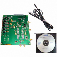
Page 51
... ADL5370 ON-BOARD QUADRATURE MODULATOR The evaluation board contains an Analog Devices, Inc., ADL5370 quadrature modulator. The AD9114/AD9115/ AD9116/AD9117 and the ADL5370 provide an easy-to-interface DAC/modulator combination that can be easily characterized on the evaluation board. Solderable jumpers can be configured to evaluate the single-ended or differential outputs of the AD9114/ AD9115/AD9116/AD9117 ...
Page 52
... AD9114/AD9115/AD9116/AD9117 EVALUATION BOARD SCHEMATICS AND ARTWORK SCHEMATICS RC0603 CC0603 RC0603 RC0603 CC0603 CC0603 Figure 111. Power Supplies and Filters Rev Page 07466-184 RC0603 CC0603 RC0603 CC0603 ...
Page 53
... RP1 DNP RNETCTS743-8 FEMALE ANGLE RIGHT Figure 112. Digital Inputs Rev Page AD9114/AD9115/AD9116/AD9117 07466-185 RNETCTS743 DNP RP5 HEADER ...
Page 54
... AD9114/AD9115/AD9116/AD9117 RC0402 RC0402 RC0402 RC0402 CC0402 CC0402 RC0402 RC0402 RC0402 Figure 113. Clock Input and DUT Rev Page 07466-186 RC0603 R7 ...
Page 55
... RC0603 RC0603 RC0603 RC0603 RC0603 RC0603 RC0603 Figure 114. IOUT Network and FSADJ1 AD9114/AD9115/AD9116/AD9117 CC0603 CC0402 RC0603 JP12 JP9 RC0603 JP8 JP7 Rev Page 07466-187 CC0805 CC0603 RC0603 RC0603 RC0603 RC0805 ERA6Y ERA6YEB323V, RC0805 ERA6Y ERA6YEB323V, RC0805 ERA6Y ERA6YEB323V, ...
Page 56
... AD9114/AD9115/AD9116/AD9117 RC0603 RC0603 RC0603 RC0603 RC0603 RC0603 RC0603 RC0603 RC0603 RC0603 Figure 115. QOUT Network and FSADJ2 Rev Page 07466-188 RC0603 JP77 RC0603 RC0603 RC0805 JP20 ERA6Y ERA6YEB323V, RC0805 JP16 ERA6Y ERA6YEB323V, RC0805 JP21 ERA6Y ERA6YEB323V, ...
Page 57
... GRN S3 S1 MLX-0532610571 Figure 116. SPI Port Rev Page AD9114/AD9115/AD9116/AD9117 07466-189 ...
Page 58
... AD9114/AD9115/AD9116/AD9117 1k RC0603 R24 C73 100PF C54 100PF ETC1-1-13 C53 100PF 1k RC0603 R61 Figure 117. Modulated Output Rev Page 07466-190 ...
Page 59
... CC0402 CC0402 HSMS-281C RC0805 Figure 118. Clock Driver Chip Rev Page AD9114/AD9115/AD9116/AD9117 07466-191 ...
Page 60
... AD9114/AD9115/AD9116/AD9117 SILKSCREENS Figure 119. Layer 2, Ground Plane Rev Page ...
Page 61
... AD9114/AD9115/AD9116/AD9117 Figure 120. Layer 3, Power Plane Rev Page ...
Page 62
... AD9114/AD9115/AD9116/AD9117 Figure 121. Assembly—Primary Side Rev Page ...
Page 63
... AD9114/AD9115/AD9116/AD9117 Figure 122. Assembly—Secondary Side Rev Page ...
Page 64
... AD9114/AD9115/AD9116/AD9117 Figure 123. Solder Mask—Primary Side with Socket Rev Page ...
Page 65
... AD9114/AD9115/AD9116/AD9117 Figure 124. Solder Mask—Secondary Side Rev Page ...
Page 66
... AD9114/AD9115/AD9116/AD9117 Figure 125. Hard Gold Plated with Bumps and Socket Rev Page ...
Page 67
... AD9114/AD9115/AD9116/AD9117 Figure 126. Primary Side Paste Rev Page ...
Page 68
... AD9114/AD9115/AD9116/AD9117 Figure 127. Secondary Side Paste Rev Page ...
Page 69
... AD9114/AD9115/AD9116/AD9117 Figure 128. Silkscreen—Primary Side Rev Page ...
Page 70
... AD9114/AD9115/AD9116/AD9117 Figure 129. Silkscreen—Secondary Side Rev Page ...
Page 71
... AD9114/AD9115/AD9116/AD9117 Figure 130. Layer 1—Primary Side Rev Page ...
Page 72
... AD9114/AD9115/AD9116/AD9117 Figure 131. Layer 4—Secondary Side Rev Page ...
Page 73
... AD9114/AD9115/AD9116/AD9117 Figure 132. Immersion Gold, No Socket, No Bumps Rev Page ...
Page 74
... AD9114/AD9115/AD9116/AD9117 Figure 133. Solder Mask—Primary Side, No Socket Rev Page ...
Page 75
... JP16, JP20, JP21, JP28, JP77 10 JP6, JP10, JP15, JP22, JP26, JPRBLK03 JP29, JP54, JP78, JP88, JP89 10 JP32, JP33, JP34, JP35, JP55, JPRSLD02 JP56, JP76, JP82, JP90, JP91 AD9114/AD9115/AD9116/AD9117 Package Description ACASE 10 μF, 6.3 V capacitor CC0603 0.1 μF capacitor CC0603 1 μF capacitor ...
Page 76
... AD9114/AD9115/AD9116/AD9117 Qty Reference Designator Device 11 L1, L2, L3, L4, L5, L6, L7, L12, IND1812 L13, L16, L19 4 L8, L9, L10, L11 IND1008 4 L14, L17, L18, L20 IND1008 1 L15 IND1210 1 P1 USB-MINIB 1 P3 Molex 0532610571 2 R1, R58 RC0805 5 R2, R23, R25, R31, R36 RC0603 5 R3, R4, R5, R10, R29 ...
Page 77
... U5, U14 ADG3304BRUZ 1 U8 74LVC1G34 1 U9 ADL5370 1 U10 AD9512 1 U12 OSC-S1703 1 U13 8-lead SOIC, ADA4899 ABM3B-20.000MHZ-10-1-U-T AD9114/AD9115/AD9116/AD9117 Package Description RNETCTS743-8 22 Ω resistor OMRONB3SG B3S-1100 push-button MINI_CD542 DNP SM-22 M/A COM ETC1-1-13 MINI_CD542 ADT9-1T MINI_BH292 JTX-4-10T+ LOOPMINI White test point LOOPMINI DNP LOOPMINI ...
Page 78
... AD9116BCPZRL7 −40°C to +85°C AD9117BCPZ 1 −40°C to +85°C 1 AD9117BCPZRL7 −40°C to +85°C AD9114-EBZ 1 1 AD9115-EBZ 1 AD9116-EBZ 1 AD9117-EBZ RoHS Compliant Part. 6.00 BSC SQ 0.60 MAX 0.50 TOP BSC 5.75 VIEW BSC SQ 0.50 0.40 0.30 0.80 MAX 0.65 TYP ...
Page 79
... NOTES AD9114/AD9115/AD9116/AD9117 Rev Page ...
Page 80
... AD9114/AD9115/AD9116/AD9117 NOTES ©2008–2009 Analog Devices, Inc. All rights reserved. Trademarks and registered trademarks are the property of their respective owners. D07466-0-3/09(A) Rev Page ...