CDB4344 Cirrus Logic Inc, CDB4344 Datasheet - Page 3
CDB4344
Manufacturer Part Number
CDB4344
Description
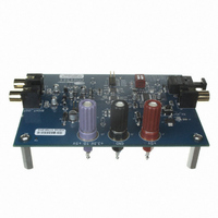
BOARD EVAL FOR CS4344 DAC
Manufacturer
Cirrus Logic Inc
Series
Popguard®r
Specifications of CDB4344
Number Of Dac's
2
Number Of Bits
24
Outputs And Type
2, Single Ended
Sampling Rate (per Second)
192k
Data Interface
Serial
Dac Type
Voltage
Voltage Supply Source
Analog and Digital
Operating Temperature
-10°C ~ 85°C
Utilized Ic / Part
CS4344
Description/function
Audio D/A
Operating Supply Voltage
5 V
Product
Audio Modules
For Use With/related Products
CS4344
Lead Free Status / RoHS Status
Contains lead / RoHS non-compliant
Lead Free Status / RoHS Status
Lead free / RoHS Compliant, Contains lead / RoHS non-compliant
Other names
598-1006


CDB4344
CDB4344 SYSTEM OVERVIEW
The CDB4344 evaluation board is an excellent means of quickly evaluating the CS4344. The
CS8416 digital audio interface receiver provides an easy interface to digital audio signal sources
including the majority of digital audio test equipment. The evaluation board also allows the user
to supply external PCM clocks and data through a header for system development.
The CDB4344 schematic has been partitioned into 4 schematics shown in Figures 2 through 5.
Each partitioned schematic is represented in the system diagram shown in Figure 1. Notice that
the system diagram also includes the interconnections between the partitioned schematics.
1. CS4344 DIGITAL TO ANALOG CONVERTER
A description of the CS4344 is included in the CS4344 datasheet.
2. CS8416 DIGITAL AUDIO RECEIVER
The system receives and decodes the standard S/PDIF data format using a CS8416 Digital Au-
dio Receiver, Figure 3. The outputs of the CS8416 include a serial bit clock, serial data, left-right
2
clock, and a 128/256 Fs master clock. The CS8416 data format is fixed to I
S (can be changed
with R42 and R47). The operation of the CS8416 and a discussion of the digital audio interface
is included in the CS8416 datasheet.
The evaluation board has been designed such that the input can be either optical or coax, see
Figure 3. However, both inputs cannot be driven simultaneously.
The right hand switch of S2 sets the output MCLK to LRCK ratio of the CS8416. This switch
should be set to 256 (closed) for inputs Fs<=96 kHz and 128 (open) for Fs>=64 kHz. The 8416
must be manually reset using RX_RST (S1) when this switch is changed.
3. INPUT FOR CLOCKS AND DATA
The evaluation board has been designed to allow interfacing to external systems via the header
J9. Header J9 allows the evaluation board to accept externally generated PCM clocks and data.
The schematic for the clock/data input is shown in Figure 4. The left hand switch of S2 selects
the source as either CS8416 (closed) or header J9 (open).
Please see the CS4344 datasheet for more information.
4. POWER SUPPLY CIRCUITRY
Power is supplied to the evaluation board by three binding posts (GND, +5V, and ‘+3.3V to +5V’),
see Figure 5. The ‘+3.3V to +5V’ which supplies VA can be jumpered to a +3.3 V regulator or the
+5V binding post. The VA supply should be set to the recommended values stated in the CS4344
datasheet.
WARNING: Refer to the CS4344 datasheet for maximum allowable voltages levels. Operation
outside of this range can cause permanent damage to the device.
DS613DB2
3
Related parts for CDB4344
Image
Part Number
Description
Manufacturer
Datasheet
Request
R

Part Number:
Description:
Development Kit
Manufacturer:
Cirrus Logic Inc
Datasheet:
Part Number:
Description:
Development Kit
Manufacturer:
Cirrus Logic Inc
Datasheet:


Part Number:
Description:
High-efficiency PFC + Fluorescent Lamp Driver Reference Design
Manufacturer:
Cirrus Logic Inc
Datasheet:
Part Number:
Description:
Development Kit
Manufacturer:
Cirrus Logic Inc
Datasheet:
Part Number:
Description:
Development Kit
Manufacturer:
Cirrus Logic Inc
Datasheet:

Part Number:
Description:
Development Kit
Manufacturer:
Cirrus Logic Inc
Datasheet:
Part Number:
Description:
Development Kit
Manufacturer:
Cirrus Logic Inc
Datasheet:
Part Number:
Description:
Development Kit
Manufacturer:
Cirrus Logic Inc
Datasheet:
Part Number:
Description:
Development Kit
Manufacturer:
Cirrus Logic Inc
Datasheet:

Part Number:
Description:
EVALUATION BOARD FOR CS8427
Manufacturer:
Cirrus Logic Inc
Datasheet:

Part Number:
Description:
BOARD EVAL FOR CS8416 RCVR
Manufacturer:
Cirrus Logic Inc
Datasheet:

Part Number:
Description:
EVALUATION BOARD FOR CS8420
Manufacturer:
Cirrus Logic Inc
Datasheet:

Part Number:
Description:
KIT DEVELOPMENT EP9315 ARM9
Manufacturer:
Cirrus Logic Inc
Datasheet:

Part Number:
Description:
KIT DEVELOPMENT EP9302 ARM9
Manufacturer:
Cirrus Logic Inc
Datasheet: