EVAL-AD5443-DBRDZ Analog Devices Inc, EVAL-AD5443-DBRDZ Datasheet - Page 14
EVAL-AD5443-DBRDZ
Manufacturer Part Number
EVAL-AD5443-DBRDZ
Description
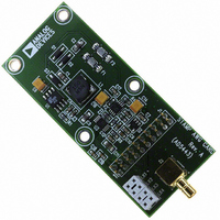
BOARD EVAL CARD CLINUX/STAMP
Manufacturer
Analog Devices Inc
Datasheet
1.AD5443YRMZ.pdf
(28 pages)
Specifications of EVAL-AD5443-DBRDZ
Number Of Dac's
1
Number Of Bits
12
Outputs And Type
1, Differential
Sampling Rate (per Second)
2.5M
Data Interface
Serial
Settling Time
50ns
Dac Type
Current
Voltage Supply Source
Single
Operating Temperature
-40°C ~ 125°C
Utilized Ic / Part
AD5443
Silicon Manufacturer
Analog Devices
Application Sub Type
DAC
Kit Application Type
Data Converter
Silicon Core Number
AD5443
Kit Contents
Board
Development Tool Type
Hardware - Eval/Demo Board
Rohs Compliant
Yes
Lead Free Status / RoHS Status
Lead free / RoHS Compliant


AD5426/AD5432/AD5443
TERMINOLOGY
Relative Accuracy
Relative accuracy or endpoint nonlinearity is a measure of the
maximum deviation from a straight line passing through the
endpoints of the DAC transfer function. It is measured after
adjusting for 0 and full scale and is normally expressed in LSBs
or as a percentage of full-scale reading.
Differential Nonlinearity
Differential nonlinearity is the difference between the measured
change and the ideal 1 LSB change between any two adjacent
codes. A specified differential nonlinearity of −1 LSB maximum
over the operating temperature range ensures monotonicity.
Gain Error
Gain error or full-scale error is a measure of the output error
between an ideal DAC and the actual device output. For these
DACs, ideal maximum output is V
DACs is adjustable to 0 with external resistance.
Output Leakage Current
Output leakage current is current that flows in the DAC ladder
switches when these are turned off. For the I
can be measured by loading all 0s to the DAC and measuring
the I
when the DAC is loaded with all 1s.
Output Capacitance
Capacitance from I
Output Current Settling Time
This is the amount of time it takes for the output to settle to a
specified level for a full-scale input change. For these devices, it
is specified with a 100 Ω resistor to ground.
The settling time specification includes the digital delay from
SYNC rising edge to the full-scale output charge.
Digital-to-Analog Glitch Impulse
The amount of charge injected from the digital inputs to the
analog output when the inputs change state. This is normally
specified as the area of the glitch in either pA-s or nV-s
depending upon whether the glitch is measured as a current
or voltage signal.
OUT
1 current. Minimum current flows in the I
OUT
1 or I
OUT
2 to AGND.
REF
− 1 LSB. Gain error of the
OUT
1 terminal, it
OUT
2 line
Rev. C | Page 14 of 28
Digital Feedthrough
When the device is not selected, high frequency logic activity
on the device digital inputs may be capacitively coupled to show
up as noise on the I
circuitry. This noise is digital feedthrough.
Multiplying Feedthrough Error
This is the error due to capacitive feedthrough from the DAC
reference input to the DAC I
loaded to the DAC.
Total Harmonic Distortion (THD)
The DAC is driven by an ac reference. The ratio of the rms sum
of the harmonics of the DAC output to the fundamental value is
the THD. Usually only the lower order harmonics are included,
such as second to fifth.
Digital Intermodulation Distortion
Second-order intermodulation distortion (IMD) measurements
are the relative magnitude of the fa and fb tones generated
digitally by the DAC and the second-order products at 2fa − fb
and 2fb − fa.
Spurious-Free Dynamic Range (SFDR)
SFDR is the usable dynamic range of a DAC before spurious
noise interferes or distorts the fundamental signal. It is the mea-
sure of the difference in amplitude between the fundamental
and the largest harmonically or nonharmonically related spur
from dc to full Nyquist bandwidth (half the DAC sampling rate,
or f
arbitrary window size, in this case 50% of the fundamental.
Digital SFDR is a measure of the usable dynamic range of the
DAC when the signal is a digitally generated sine wave.
S
/2). Narrow band SFDR is a measure of SFDR over an
THD
=
20
log
OUT
(
V
pins and subsequently into the following
2
2
+
V
OUT
3
2
V
1 terminal, when all 0s are
+
1
V
4
2
+
V
5
2
)
Related parts for EVAL-AD5443-DBRDZ
Image
Part Number
Description
Manufacturer
Datasheet
Request
R

Part Number:
Description:
IC, ADJ LDO REG, 1.5V TO 5V 250mA MSOP-8
Manufacturer:
Vishay
Datasheet:

Part Number:
Description:
IC, ADJ LDO REG, 1.5V TO 5V 0.6A 8-TSSOP
Manufacturer:
Vishay
Datasheet:
Part Number:
Description:
IC, ADJ LDO REG, 1.5V TO 5V 250mA MSOP-8
Manufacturer:
Vishay
Datasheet:

Part Number:
Description:
IC ADJ LDO REG 1.5V TO 5V 150mA 5-SOT-23
Manufacturer:
Vishay
Datasheet:

Part Number:
Description:
BOARD EVAL AS1324-AD
Manufacturer:
austriamicrosystems
Datasheet:
Part Number:
Description:
IC, ADJ LDO REG, 1.5V TO 5V 0.6A 8-TSSOP
Manufacturer:
Vishay
Datasheet:

Part Number:
Description:
IC, ADJ LDO REG, 1.5V TO 5V, 0.3A, MSOP8
Manufacturer:
Vishay
Datasheet:
Part Number:
Description:
IC, ADJ LDO REG, 1.5V TO 5V, 0.3A, MSOP8
Manufacturer:
Vishay
Datasheet:
Part Number:
Description:
IC, ADJ LDO REG 1.215V TO 5V 0.3A MSOP-8
Manufacturer:
Vishay
Datasheet:
Part Number:
Description:
IC, ADJ LDO REG 1.215V TO 5V 0.3A MSOP-8
Manufacturer:
Vishay
Datasheet:

Part Number:
Description:
±1.7g Dual-Axis IMEMS Accelerometer Evaluation Board
Manufacturer:
Analog Devices Inc
Datasheet:

Part Number:
Description:
IC MULTIPLIER ANALOG 8-SOIC T/R
Manufacturer:
Analog Devices Inc
Datasheet:

Part Number:
Description:
IC ANALOG MULTIPLIER 8-DIP
Manufacturer:
Analog Devices Inc
Datasheet:
Part Number:
Description:
IC ANALOG MULTIPLIER 8-SOIC
Manufacturer:
Analog Devices Inc
Datasheet:
Part Number:
Description:
IC ANALOG MULTIPLIER 8-DIP
Manufacturer:
Analog Devices Inc
Datasheet: