EVAL-AD5821EBZ Analog Devices Inc, EVAL-AD5821EBZ Datasheet - Page 11
EVAL-AD5821EBZ
Manufacturer Part Number
EVAL-AD5821EBZ
Description
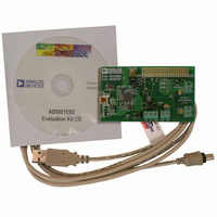
BOARD EVALUATION FOR AD5821
Manufacturer
Analog Devices Inc
Datasheet
1.AD5821ABCBZ-REEL7.pdf
(16 pages)
Specifications of EVAL-AD5821EBZ
Number Of Dac's
1
Number Of Bits
10
Outputs And Type
1, Single Ended
Sampling Rate (per Second)
400k
Data Interface
I²C
Settling Time
250µs
Dac Type
Current
Voltage Supply Source
Single
Operating Temperature
-30°C ~ 80°C
Utilized Ic / Part
AD5821
Lead Free Status / RoHS Status
Lead free / RoHS Compliant


THEORY OF OPERATION
The AD5821 is a fully integrated, 10-bit digital-to-analog
converter (DAC) with 120 mA output current sink capability.
It is intended for driving voice coil actuators in applications
such as lens autofocus, image stabilization, and optical zoom.
The circuit diagram is shown in Figure 20. A 10-bit current
output DAC coupled with Resistor R generates the voltage that
drives the noninverting input of the operational amplifier. This
voltage also appears across the R
sink current required to drive the voice coil.
Resistor R and Resistor R
Therefore, the temperature coefficient and any nonlinearities
over temperature are matched, and the output drift over tempera-
ture is minimized. Diode D1 is an output protection diode.
SERIAL INTERFACE
The AD5821 is controlled using the industry-standard I
2-wire serial protocol. Data can be written to or read from the
DAC at data rates of up to 400 kHz. After a read operation, the
contents of the input register are reset to all 0s.
I
An I
generate the serial clock (SCL) and read and write data on the
serial data line (SDA) to and from slave devices such as the
AD5821. All devices on an I
to the SDA line and their SCL pin connected to the SCL line of
the master device. I
pulling high is achieved by pull-up resistors, R
depends on the data rate, bus capacitance, and the maximum load
current that the I
1.8V
SDA
SCL
2
R
C BUS OPERATION
P
2
C bus operates with one or more master devices that
R
P
Figure 20. Block Diagram Showing Connection to Voice Coil
INTERFACE
I
2
C SERIAL
SDA
SCL
DGND
I
2
C MASTER
DEVICE
2
C device can sink (3 mA for a standard device).
2
AD5821
C devices can only pull the bus lines low;
REFERENCE
OUTPUT DAC
XSHUTDOWN
Figure 21. Typical I
CURRENT
10-BIT
I
SENSE
2
DEVICE
C SLAVE
2
C bus have their SDA pin connected
are interleaved and matched.
POWER-ON
SENSE
RESET
R
resistor and generates the
2
C Bus
V
AD5821
DD
R
SENSE
P
DGND
3.3Ω
. The value of R
AGND
D1
I
2
DEVICE
C SLAVE
V
DD
2
C
I
SINK
Rev. 0 | Page 11 of 16
P
When the bus is idle, SCL and SDA are both high. The master
device initiates a serial bus operation by generating a start
condition, which is defined as a high-to-low transition on the
SDA low while SCL is high. The slave device connected to the
bus responds to the start condition and shifts in the next eight
data bits under control of the serial clock. These eight data bits
consist of a 7-bit address, plus a read/write (R/ W ) bit that is 0 if
data is to be written to a device, and 1 if data is to be read from a
device. Each slave device on an I
The address of the AD5821 is 0001100; however, 0001101,
0001110, and 0001111 address the part because the last two bits
are unused/don’t cares (see Figure 22 and Figure 23). Because the
address plus the R/ W bit always equals eight bits of data, the write
address of the AD5821 is 00011000 (0x18) and the read address
is 00011001 (0x19) (see Figure 22 and Figure 23).
At the end of the address data, after the R/ W bit, the slave
device that recognizes its own address responds by generating
an acknowledge (ACK) condition. This is defined as the slave
device pulling SDA low while SCL is low before the ninth clock
pulse and keeping it low during the ninth clock pulse. Upon
receiving ACK, the master device can clock data into the AD5821
in a write operation, or it can clock it out in a read operation.
Data must change either during the low period of the clock
(because SDA transitions during the high period define a start
condition, as described previously), or during a stop condition,
as described in the Data Format section.
I
an ACK at the end of each block. Because the AD5821 requires
10 bits of data, two data-words must be written to it when a
write operation occurs, or read from it when a read operation
occurs. At the end of a read or write operation, the AD5821
acknowledges the second data byte. The master generates a stop
condition, defined as a low-to-high transition on SDA while SCL
is high, to end the transaction.
DATA FORMAT
Data is written to the AD5821 high byte first, MSB first, and is
shifted into the 16-bit input register. After all data is shifted in,
data from the input register is transferred to the DAC register.
Because the DAC requires only 10 bits of data, not all bits of the
input register data are used. The MSB is reserved for an active-
high, software-controlled, power-down function. Bit 14 is unused;
Bit 13 to Bit 4 correspond to the DAC data bits, Bit 9 to Bit 0.
Bit 3 to Bit 0 are unused.
During a read operation, data is read in the same bit order.
2
C data is divided into blocks of eight bits, and the slave generates
2
C bus must have a unique address.
AD5821
Related parts for EVAL-AD5821EBZ
Image
Part Number
Description
Manufacturer
Datasheet
Request
R


Part Number:
Description:
BOARD EVAL FOR SI270X-A
Manufacturer:
Silicon Laboratories Inc
Datasheet:

Part Number:
Description:
BUCK CONV REF DESIGN KIT IP1201
Manufacturer:
International Rectifier
Datasheet:
Part Number:
Description:
BOARD DEMO SYNC DUAL BUCK CNVTER
Manufacturer:
International Rectifier
Datasheet:
Part Number:
Description:
BOARD DEMO SYNC BUCK CONVETER
Manufacturer:
International Rectifier
Datasheet:

Part Number:
Description:
EVALBOARD/EB Omnidirectional microphone - Analog
Manufacturer:
Analog Devices
Datasheet:
Part Number:
Description:
EVALBOARD/EB Omnidirectional microphone - Analog
Manufacturer:
Analog Devices
Datasheet:


Part Number:
Description:
BOARD EVAL LED DRIVER LT3756
Manufacturer:
Linear Technology
Datasheet:

Part Number:
Description:
BOARD EVAL FOR AD7741/7742
Manufacturer:
Analog Devices Inc
Datasheet:

Part Number:
Description:
±1.7g Dual-Axis IMEMS Accelerometer Evaluation Board
Manufacturer:
Analog Devices Inc
Datasheet:

Part Number:
Description:
IC MULTIPLIER ANALOG 8-SOIC T/R
Manufacturer:
Analog Devices Inc
Datasheet:

Part Number:
Description:
IC ANALOG MULTIPLIER 8-DIP
Manufacturer:
Analog Devices Inc
Datasheet:
Part Number:
Description:
IC ANALOG MULTIPLIER 8-SOIC
Manufacturer:
Analog Devices Inc
Datasheet:
Part Number:
Description:
IC ANALOG MULTIPLIER 8-DIP
Manufacturer:
Analog Devices Inc
Datasheet: