EVAL-AD5415EBZ Analog Devices Inc, EVAL-AD5415EBZ Datasheet - Page 5
EVAL-AD5415EBZ
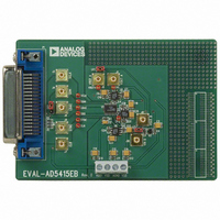
Manufacturer Part Number
EVAL-AD5415EBZ
Description
BOARD EVALUATION FOR AD5415
Manufacturer
Analog Devices Inc
Specifications of EVAL-AD5415EBZ
Number Of Dac's
2
Number Of Bits
12
Outputs And Type
2, Differential
Sampling Rate (per Second)
2.47M
Data Interface
Serial
Settling Time
120ns
Dac Type
Current
Voltage Supply Source
Single
Operating Temperature
-40°C ~ 125°C
Utilized Ic / Part
AD5415
Lead Free Status / RoHS Status
Lead free / RoHS Compliant


TIMING CHARACTERISTICS
All input signals are specified with tr = tf = 1 ns (10% to 90% of V
V
Table 2.
Parameter
f
t
t
t
t
t
t
t
t
t
t
t
t
Update Rate
1
2
3
SCLK
1
2
3
4
5
6
7
8
9
10
11
12
Guaranteed by design and characterization, not subject to production test.
Falling or rising edge as determined by the control bits of the serial word. Strong or weak SDO driver selected via the control register.
Daisy-chain and readback modes cannot operate at maximum clock frequency. SDO timing specifications measured with a load circuit, as shown in Figure 5.
REF
3
= 10 V, I
1
OUT
1
2
NOTES
ALTERNATIVELY, DATA CAN BE CLOCKED INTO THE INPUT SHIFT REGISTER ON THE RISING EDGE OF SCLK AS
DETERMINED BY THE CONTROL BITS. TIMING IS AS ABOVE, WITH SCLK INVERTED.
LDAC
LDAC
SYNC
ASYNCHRONOUS LDAC UPDATE MODE.
SYNCHRONOUS LDAC UPDATE MODE.
SCLK
2 = 0 V, temperature range for Y version: −40°C to +125°C. All specifications T
DIN
Limit at T
50
20
8
8
13
5
4
5
30
0
12
10
25
60
2.47
1
2
t
8
MIN
, T
t
4
MAX
DB15
t
5
Unit
MHz max
ns min
ns min
ns min
ns min
ns min
ns min
ns min
ns min
ns min
ns min
ns min
ns min
ns min
MSPS
t
6
Figure 2. Standalone Mode Timing Diagram
t
2
Conditions/Comments
Maximum clock frequency
SCLK cycle time
SCLK high time
SCLK low time
SYNC falling edge to SCLK falling edge setup time
Data setup time
Data hold time
SYNC rising edge to SCLK falling edge
Minimum SYNC high time
SCLK falling edge to LDAC falling edge
LDAC pulse width
SCLK falling edge to LDAC rising edge
SCLK active edge to SDO valid, strong SDO driver
SCLK active edge to SDO valid, weak SDO driver
Consists of cycle time, SYNC high time, data setup, and output voltage settling time
Rev. B | Page 5 of 32
t
1
DD
t
3
) and timed from a voltage level of (V
DB0
t
7
t
9
2
t
10
t
11
MIN
to T
MAX
IL
, unless otherwise noted.
+ V
IH
)/2. V
DD
= 2.5 V to 5.5 V,
AD5415
Related parts for EVAL-AD5415EBZ
Image
Part Number
Description
Manufacturer
Datasheet
Request
R


Part Number:
Description:
BOARD EVAL FOR SI270X-A
Manufacturer:
Silicon Laboratories Inc
Datasheet:

Part Number:
Description:
BUCK CONV REF DESIGN KIT IP1201
Manufacturer:
International Rectifier
Datasheet:
Part Number:
Description:
BOARD DEMO SYNC DUAL BUCK CNVTER
Manufacturer:
International Rectifier
Datasheet:
Part Number:
Description:
BOARD DEMO SYNC BUCK CONVETER
Manufacturer:
International Rectifier
Datasheet:

Part Number:
Description:
EVALBOARD/EB Omnidirectional microphone - Analog
Manufacturer:
Analog Devices
Datasheet:
Part Number:
Description:
EVALBOARD/EB Omnidirectional microphone - Analog
Manufacturer:
Analog Devices
Datasheet:


Part Number:
Description:
BOARD EVAL LED DRIVER LT3756
Manufacturer:
Linear Technology
Datasheet:

Part Number:
Description:
BOARD EVAL FOR AD7741/7742
Manufacturer:
Analog Devices Inc
Datasheet:

Part Number:
Description:
±1.7g Dual-Axis IMEMS Accelerometer Evaluation Board
Manufacturer:
Analog Devices Inc
Datasheet:

Part Number:
Description:
IC MULTIPLIER ANALOG 8-SOIC T/R
Manufacturer:
Analog Devices Inc
Datasheet:

Part Number:
Description:
IC ANALOG MULTIPLIER 8-DIP
Manufacturer:
Analog Devices Inc
Datasheet:
Part Number:
Description:
IC ANALOG MULTIPLIER 8-SOIC
Manufacturer:
Analog Devices Inc
Datasheet:
Part Number:
Description:
IC ANALOG MULTIPLIER 8-DIP
Manufacturer:
Analog Devices Inc
Datasheet: