LM3503ITL-25EV National Semiconductor, LM3503ITL-25EV Datasheet - Page 8
LM3503ITL-25EV
Manufacturer Part Number
LM3503ITL-25EV
Description
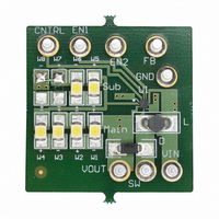
BOARD EVALUATION LM3503ITL-25
Manufacturer
National Semiconductor
Series
PowerWise®r
Specifications of LM3503ITL-25EV
Current - Output / Channel
9mA
Outputs And Type
2, Non-Isolated
Voltage - Output
25 V
Features
Dual Display(s)
Voltage - Input
2.7 ~ 5.5V
Utilized Ic / Part
LM3503
Core Chip
LM3503
Topology
Boost
No. Of Outputs
1
Output Voltage
25V
Input Voltage
2.5V To 5.5V
Development Tool Type
Hardware - Eval/Demo Board
Lead Free Status / RoHS Status
Not applicable / Not applicable


www.national.com
Detailed Description of Operation
The LM3503 utilizes an asynchronous current mode pulse-
width-modulation (PWM) control scheme to regulate the
feedback voltage over specified load conditions. The DC/DC
converter behaves as a controlled current source for white
LED applications. The operation can best be understood by
referring to the block diagram in Figure 1 for the following
operational explanation. At the start of each cycle, the oscil-
lator sets the driver logic and turns on the internal NMOS
power device, N1, conducting current through the inductor
and reverse biasing the external diode. The white LED cur-
rent is supplied by the output capacitor when the internal
NMOS power device, N1, is turned on. The sum of the error
amplifier’s output voltage and an internal voltage ramp are
compared with the sensed power NMOS, N1, switch voltage.
Once these voltages are equal, the PWM comparator will
then reset the driver logic, thus turning off the internal NMOS
power device, N1, and forward biasing the external diode.
The inductor current then flows through the diode to the
white LED load and output capacitor. The inductor current
recharges the output capacitor and supplies the current for
the white LED load. The oscillator then sets the driver logic
again repeating the process. The output voltage of the error
amplifier controls the current through the inductor. This volt-
age will increase for larger loads and decrease for smaller
loads limiting the peak current in the inductor and minimizing
EMI radiation. The duty limit comparator is always opera-
tional, it prevents the internal NMOS power switch, N1, from
being on for more than one oscillator cycle and conducting
large amounts of current. The light load comparator allows
the LM3503 to properly regulate light/small white LED load
currents, where regulation becomes difficult for the
LM3503’s primary control loop. Under light load conditions,
the LM3503 will enter into a pulse skipping pulse-frequency-
mode (PFM) of operation where the operational frequency
will vary with the load. As a result of PFM mode operation,
the output voltage ripple magnitude will significantly in-
crease.
The LM3503 has two control pins, En1 and En2, used for
selecting which segment of a single white LED string net-
FIGURE 2. Operational Characteristics Table
8
work is active for dual display applications. En1 controls the
main display (MAIN) segment of the single string white LED
network between pins V
sub display (SUB) segment of the single string white LED
network between the V
are ≤ 0.3V, the LM3503 will shutdown, for further description
of the En1 and En2 operation, see Figure 3. During shut-
down the output capacitor discharges through the string of
white LEDs and feedback resistor to ground. The LED cur-
rent can be dynamically controlled by a DC voltage on the
Cntrl pin. When V
equal to zero because of offsets within the LM3503 internal
circuitry. To guarantee zero white LED current the LM3503
must be in shutdown mode operation.
The LM3503 has dedicated protection circuitry active during
normal operation to protect the integrated circuit (IC) and
external components. Soft start circuitry is present in the
LM3503 to allow for slowly increasing the current limit to its
steady-state value to prevent undesired high inrush current
during start up. Thermal shutdown circuitry turns off the
internal NMOS power device, N1, when the internal semi-
conductor junction temperature reaches excessive levels.
The LM3503 has a under-voltage protection (UVP) compara-
tor that disables the internal NMOS power device when
battery voltages are too low, thus preventing an on state
where the internal NMOS power device conducts large
amounts of current. The over-voltage protection (OVP) com-
parator prevents the output voltage from increasing beyond
the protection limit when the white LED string network is
removed or if there is a white LED failure. OVP allows for the
use of low profile ceramic capacitors at the output. The
current through the internal NMOS power device, N1, is
monitored to prevent peak inductor currents from damaging
the IC. If during a cycle (cycle=1/switching frequency) the
peak inductor current exceeds the current limit for the
LM3503, the internal NMOS power device will be turned off
for the remaining duration of that cycle.
Cntrl
= 0V the white LED current may not be
OUT2
OUT1
and Fb. If both V
and V
OUT2
20128605
. En2 controls the
En1
and V
En2
Related parts for LM3503ITL-25EV
Image
Part Number
Description
Manufacturer
Datasheet
Request
R

Part Number:
Description:
IC LED DRVR WHT BCKLT 10MICROSMD
Manufacturer:
National Semiconductor
Datasheet:
Part Number:
Description:
IC LED DRVR WHT BCKLT 10MICROSMD
Manufacturer:
National Semiconductor
Datasheet:
Part Number:
Description:
IC LED DRVR WHT BCKLT 10MICROSMD
Manufacturer:
National Semiconductor
Datasheet:
Part Number:
Description:
IC LED DRVR WHT BCKLT 10MICROSMD
Manufacturer:
National Semiconductor
Datasheet:

Part Number:
Description:
IC, LED DRIVER, CONSTANT CURRENT, µSMD16
Manufacturer:
National Semiconductor
Datasheet:

Part Number:
Description:
Dual-Display Constant Current LED Driver with Analog Brightness Control
Manufacturer:
National Semiconductor
Datasheet:
Part Number:
Description:
LM3503 Dual-Display Constant Current LED Driver with Analog Brightness Control; Package: MICRO SMD; No of Pins: 10; Qty per Container: 250; Container: Reel
Manufacturer:
National Semiconductor
Datasheet:
Part Number:
Description:
National Semiconductor [8-Bit D/A Converter]
Manufacturer:
National Semiconductor
Datasheet:
Part Number:
Description:
National Semiconductor [Media Coprocessor]
Manufacturer:
National Semiconductor
Datasheet:
Part Number:
Description:
Digitally Controlled Tone and Volume Circuit with Stereo Audio Power Amplifier, Microphone Preamp Stage and National 3D Sound
Manufacturer:
National Semiconductor
Datasheet:
Part Number:
Description:
Digitally Controlled Tone and Volume Circuit with Stereo Audio Power Amplifier, Microphone Preamp Stage and National 3D Sound
Manufacturer:
National Semiconductor
Datasheet:
Part Number:
Description:
AC97 Rev 2 Codec with Sample Rate Conversion and National 3D Sound
Manufacturer:
National Semiconductor
Part Number:
Description:
Manufacturer:
National Semiconductor
Datasheet:
Part Number:
Description:
Manufacturer:
National Semiconductor
Datasheet: