AD8337-EVALZ Analog Devices Inc, AD8337-EVALZ Datasheet - Page 18
AD8337-EVALZ
Manufacturer Part Number
AD8337-EVALZ
Description
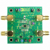
BOARD EVALUATION FOR AD8337
Manufacturer
Analog Devices Inc
Series
X-AMP®r
Specifications of AD8337-EVALZ
Channels Per Ic
1 - Single
Amplifier Type
Voltage Feedback
Output Type
Single-Ended
Slew Rate
625 V/µs
-3db Bandwidth
280MHz
Operating Temperature
-40°C ~ 85°C
Current - Supply (main Ic)
18.5mA
Voltage - Supply, Single/dual (±)
±2.5 V ~ 5 V
Board Type
Fully Populated
Utilized Ic / Part
AD8337
Silicon Manufacturer
Analog Devices
Application Sub Type
Variable Gain Amplifier
Kit Application Type
Amplifier
Silicon Core Number
AD8337
Kit Contents
Board
Lead Free Status / RoHS Status
Lead free / RoHS Compliant
Current - Output / Channel
-
Lead Free Status / RoHS Status
Lead free / RoHS Compliant, Lead free / RoHS Compliant
Available stocks
Company
Part Number
Manufacturer
Quantity
Price
Company:

Part Number:
AD8337-EVALZ
Manufacturer:
Analog Devices Inc
Quantity:
135


AD8337
THEORY OF OPERATION
OVERVIEW
The AD8337 is a low noise, single-ended, linear-in-dB, general-
purpose variable gain amplifier (VGA) usable at frequencies up
to 100 MHz. It is fabricated using a proprietary Analog Devices
dielectrically isolated, complementary bipolar process. The
bandwidth is dc to 280 MHz and features low dc offset voltage
and an ideal nominal gain range of 0 dB to 24 dB. Requiring
about 15.5 mA, the power consumption is only 78 mW from
either a single +5 V or a dual ±2.5 V supply. Figure 65 is the
circuit block diagram of the AD8337.
PREAMPLIFIER
An uncommitted current-feedback op amp included in the
AD8337 can be used as a preamplifier to buffer the ladder
network attenuator of the X-AMP. As with any op amp, the gain
is established using external resistors, and the preamplifier is
specified with a noninverting gain of 6 dB (2×) and gain resistor
values of 100 Ω. The preamplifier gain can be increased using
larger values of R
The value of R
internal compensation capacitor determine the 3 dB bandwidth,
and smaller values can compromise preamplifier stability.
Because the AD8337 is dc-coupled, larger preamp gains increase
the offset voltage. The offset voltage can be compensated by
connecting a resistor between the INPN input and the supply
voltage. If the offset is negative, the resistor value connects to
the negative supply. For ease of adjustment, a trimmer network
can be used.
For larger gains, the overall noise is reduced if a low value of
R
preamp gain is 16× (24.1 dB), and the input-referred noise is
approximately 1.5 nV/√Hz. For this value of gain, the overall
gain range increases by 18 dB; therefore, the gain range is 18 dB
to 42 dB.
FB1
is selected. For values of R
FB2
FB2
is to be ≥100 Ω because the value and an
, trading off bandwidth and offset voltage.
FB1
R
= 20 Ω and R
G
R
R
FB1
INPP
INPN
PRAO
FB2
FB2
3
4
5
= 301 Ω, the
R
FB1
+
–
PrA
6dB
= R
BIAS
Figure 65. Circuit Block Diagram
FB2
VCOM
= 100Ω
Rev. C | Page 18 of 32
2
INTERPOLATOR
–24dB TO 0dB
+
ATTENUATOR
–
VPOS
VNEG
8
6
VGA
This X-AMP, with its linear-in-dB gain characteristic
architecture, yields the optimum dynamic range for receiver
applications. Referring to Figure 65, the signal path consists of
a −24 dB variable attenuator followed by a fixed gain amplifier of
18 dB, for a total VGA gain range of −6 dB to +18 dB. With the
preamplifier configured for a gain of 6 dB, the composite gain
range is 0 dB to 24 dB.
The VGA plus preamp, with 6 dB of gain, implements the
following exact gain law:
where the nominal intercept (ICPT) = 12.65 dB.
The ICPT increases as the gain of the preamp is increased. For
example, if the gain of the preamp is increased by 6 dB, ICPT
increases to 18.65 dB. Although the previous equation shows
the exact gain law as based on statistical data, a quick estimation
of signal levels can be made using the default slope of 20 dB/V
for a particular gain setting. For example, the change in gain for
a V
5.91 dB using the exact slope of 19.6 dB/V. This is a difference
of only 0.09 dB.
GAIN CONTROL
The gain control interface provides a high impedance input and
is referenced to the VCOM pin (in a single-supply application to
midsupply at [VPOS + VNEG]/2 for optimum swing). When
dual supplies are used, VCOM is connected to ground. The voltage
on the VCOM pin determines the midpoint of the gain range. For
a ground referenced design, the VGAIN range is from −0.7 V to
+0.7 V with the most linear-in-dB section of the gain control
between −0.6 V and +0.6 V. In the center 80% of the VGAIN
range, the gain error is typically less than ±0.2 dB. The gain
control voltage can be increased or decreased to the positive or
negative rails without gain foldover.
GAIN
Gain
change of 0.3 V is 6 dB using a slope of 20 dB/V and
INTERFACE
(dB)
+
–
18dB
(8x)
GAIN
GAIN
7
=
749Ω
107Ω
⎡
⎢ ⎣
19.7
dB
V
1
VOUT
×
V
GAIN
⎤
⎥ ⎦
+
ICPT
(dB)
Related parts for AD8337-EVALZ
Image
Part Number
Description
Manufacturer
Datasheet
Request
R

Part Number:
Description:
KIT EVAL DUAL SUPPLY INV AD8337
Manufacturer:
Analog Devices Inc
Datasheet:
Part Number:
Description:
KIT EVAL SINGLE SUPPLY AD8337
Manufacturer:
Analog Devices Inc
Datasheet:
Part Number:
Description:
RoHS Compliant Eval Board.
Manufacturer:
Analog Devices Inc
Datasheet:
Part Number:
Description:
RoHS Compliant Eval Board.
Manufacturer:
Analog Devices Inc
Datasheet:

Part Number:
Description:
±1.7g Dual-Axis IMEMS Accelerometer Evaluation Board
Manufacturer:
Analog Devices Inc
Datasheet:
Part Number:
Description:
Inertial Sensor Evaluation System
Manufacturer:
Analog Devices Inc
Datasheet:
Part Number:
Description:
Manufacturer:
Analog Devices Inc
Datasheet:
Part Number:
Description:
Manufacturer:
Analog Devices Inc
Datasheet:
Part Number:
Description:
Manufacturer:
Analog Devices Inc
Datasheet:
Part Number:
Description:
Manufacturer:
Analog Devices Inc
Datasheet:
Part Number:
Description:
Manufacturer:
Analog Devices Inc
Datasheet:
Part Number:
Description:
Manufacturer:
Analog Devices Inc
Datasheet:
Part Number:
Description:
Manufacturer:
Analog Devices Inc
Datasheet: