© 2004 National Semiconductor Corporation
General Description
The LMH730275 evaluation board is designed to aid in the
characterization of National Semiconductor’s high speed
triple SSOP operational amplifiers.
Use the evaluation board as a guide for high frequency
layout and as a tool to aid in device testing and character-
ization.
The evaluation board schematic is shown below in Figure 1.
Refer to the product data sheets for recommendations for
component values.
Basic Operation
By changing R
ances can be matched. The SMA connectors and board
traces are optimized for 50 to 75Ω operation. Other imped-
ances can be matched but performance will be noticeably
different, especially high frequency response. Even with op-
timal layout board parasitics play a large part in high fre-
quency performance and different termination resistors will
change the frequency of the dominant parasitic poles/zeros.
Inverting configuration
The evaluation board is set up for non inverting operation.
For inverting operation make the following modifications (see
Figure 4 and Figure 5): On the bottom of the board cut the
input trace just before the via to the R1 resistors and run
jumpers to the vias that connect to the ground side of R
is on the top side of the board). On the top side of the board
cut the tab between the ground plane and the grounded pad
of R
input impedance of the board it can be soldered between R
and the ground plane where the tab was cut (the board is
labeled for R
Layout Considerations
Printed circuit board layout and supply bypassing play major
roles in determining high frequency performance. When de-
signing your own board use these evaluation boards as a
guide and follow these steps to optimize high frequency
performance:
LMH730275 Triple High Speed SSOP Op Amp Evaluation
G
. An additional resistor R
T
).
IN
and R
OUT
different input and output imped-
T
can be used to lower the
MS201012
G
Board
(R
G
G
1. Use a ground plane
2. Include large ( ~ 6.8 µF) capacitors on both supplies:
3. Near the device use .01 µF ceramic capacitors from both
4. For improved bypassing .1 µF ceramic capacitors can
5. Remove the ground and power planes from under the
6. Minimize all trace lengths
7. Use terminated transmission lines for long traces.
8. 2
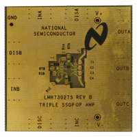
R1A, R1B and R1Care input matching resistors. ROUTA,
ROUTB and ROUTC are output matching resistors. RDA,
RDB and RDC are input matching resistors for high speed
signals applied to the disable inputs. If the disable inputs are
not used leave RDA, RDB and RDC empty. Sample artwork
for the LMH730275 Evaluation board is included on the next
page in Figure 2.
Measurement Hints
The board is designed for 50Ω input and output connections
into coaxial cables. For other impedances the terminating
resistors can be modified to help match different imped-
ances.
Do not use normal oscilloscope probes to test these circuits.
The capacitive loading will change circuit performance dras-
tically. Instead use low impedance resistive divider probes of
100 to 500Ω. See Figure 3 for a sample resistive probe. The
Low impedance resistor should be 50- 450Ω . The ground
connection should be as short as possible ( ~ 1/2”). Even with
careful use of these probes results should be considered
preliminary until verified with controlled impedance measure-
ments. Even the best probes will interfere with circuit opera-
tion to some degree. Also, tools, power cables, fingers etc.
near the device will change measurement results often
dramatically.
C5 & C6.
supplies to ground: C1-C4
be stacked on top of C1-C4.
input and output pins.
board layout and power supply bypassing experiment
with bypass capacitor values for best results.
nd
Harmonic Distortion performance is impacted by
www.national.com
April 2004